Pixel circuit, driving method of pixel circuit, and display device adopting pixel circuit

A pixel circuit and row pixel technology, applied in the field of pixel circuits and display devices, can solve the problems of large layout space, multiple control signals, etc., and achieve the effects of uniform display, reduced current density, and increased aperture ratio

Active Publication Date: 2014-11-19
BOE TECH GRP CO LTD +1
View PDF5 Cites 19 Cited by
  • Summary
  • Abstract
  • Description
  • Claims
  • Application Information

AI Technical Summary

Problems solved by technology

[0005] In the prior art, the increase in the number of TFTs and / or capacitors for threshold compensation will require more control signals and occupy a larger layout space, which is not conducive to the reduction of AMOLED pixel size, which limits the high PPI ( Pixel Per Inch, the number of pixels per inch) AMOLED pixel drive circuit development

Method used


Image

  • Pixel circuit, driving method of pixel circuit, and display device adopting pixel circuit
  • Pixel circuit, driving method of pixel circuit, and display device adopting pixel circuit
  • Pixel circuit, driving method of pixel circuit, and display device adopting pixel circuit

Examples


Embodiment Construction

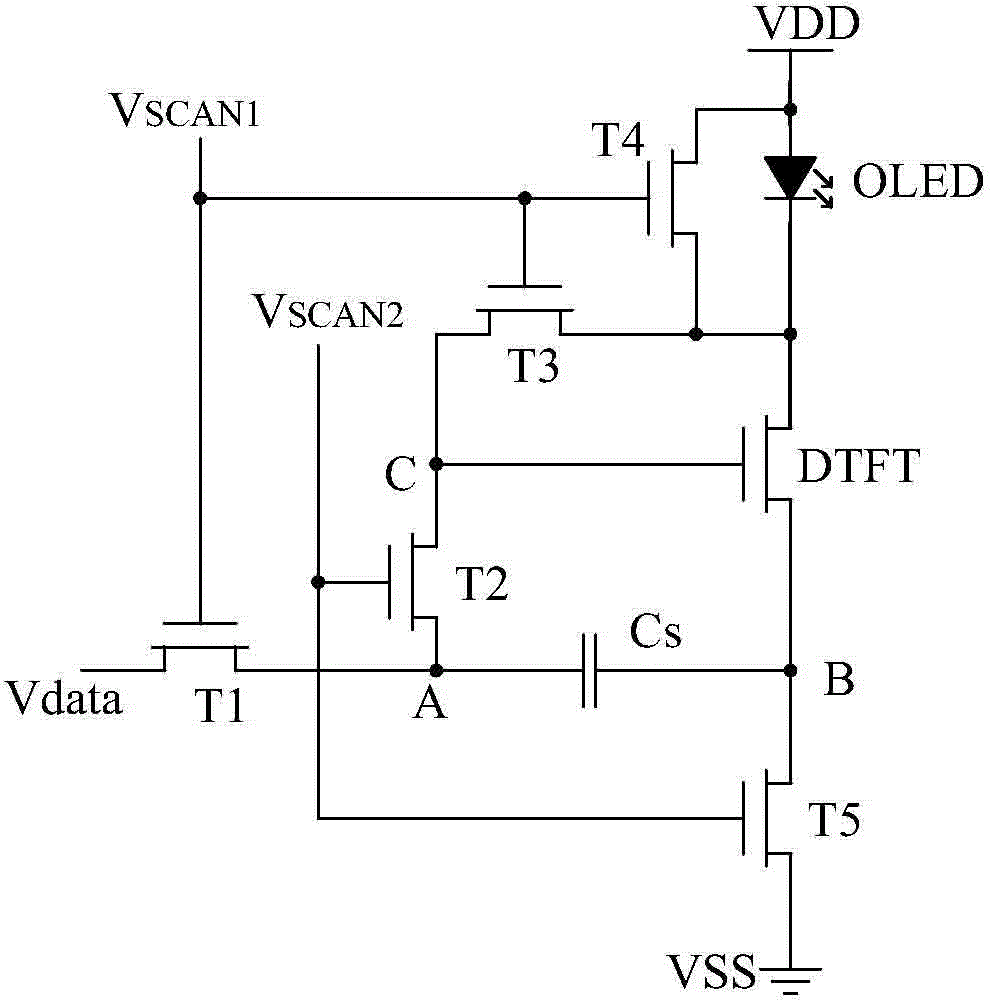
[0039] The following will clearly and completely describe the technical solutions in the embodiments of the present invention with reference to the accompanying drawings in the embodiments of the present invention. Obviously, the described embodiments are only some, not all, embodiments of the present invention. Based on the embodiments of the present invention, all other embodiments obtained by persons of ordinary skill in the art without making creative efforts belong to the protection scope of the present invention.

[0040] The transistors used in all the embodiments of the present invention can be thin film transistors or field effect transistors or other devices with the same characteristics. In the embodiment of the present invention, in order to distinguish the two poles of the transistor except the gate, the first pole may be the source or the drain, and the second pole may be the drain or the source. In addition, transistors can be classified into n-type transistors ...


PUM


Abstract

The invention provides a pixel circuit, a driving method of the pixel circuit, and a display device adopting the pixel circuit. The pixel circuit comprises a plurality of pixel unit rows; each pixel unit row comprises a plurality of sub-pixel units and further comprises a row shared unit; each sub-pixel unit comprises a light-emitting element; the row shared unit comprises a plurality of row driving light-emitting control modules; all the sub-pixel units in each pixel unit row are connected with a signal wire and a scanning line; a light-emitting control signal is accessed into each row driving light-emitting control module; the row driving light-emitting control module is connected with all the sub-pixel units of one pixel unit row through the signal wire, so as to write voltage data under the control of a scanning signal output by the scanning line, have a threshold compensation function, and then drive the light-emitting element to emit light under the control of the light-emitting control signal. The pixel circuit, the driving method and the display device have the advantages that the pixel aperture ratio is improved; the display is uniform; the current density of an organic emitting layer is reduced.

Description

technical field [0001] The present invention relates to the field of display technology, in particular to a pixel circuit, a driving method for the pixel circuit and a display device. Background technique [0002] Due to the AMOLED (Active Matrix / Organic Light Emitting Diode, Active Matrix Organic Light Emitting Diode) pixel drive circuit based on LTPS (Low Temperature Poly-silicon, low temperature polysilicon technology), due to LTPS has problems such as poor threshold voltage uniformity, so in AMOLED In pixel design, it is necessary to add a circuit for driving TFT (Thin Film Transistor, Thin Film Field Effect Transistor) threshold voltage compensation. [0003] Such as Figure 1A As shown, a common design of an AMOLED pixel driver circuit with threshold voltage compensation requires a 6T1C pixel driver circuit, or requires more TFTs and / or capacitors. Such as Figure 1A As shown, the 6T1C pixel drive circuit includes a first control transistor T1, a second control transi...

Claims


Application Information

Patent Timeline
Patent Type & Authority Applications(China)
IPC IPC(8): G09G3/32G09G3/3225
CPCG09G3/3233G09G2300/0819G09G2300/0842G09G2300/0861G09G3/3291G09G2300/0465G09G2320/0233G09G2320/043G09G3/3258G09G2300/043G09G2300/0809G09G2310/08
Inventor 吴博祁小敬谭文
Owner BOE TECH GRP CO LTD
Why Eureka
Try Eureka