

Semiconductor structure, forming method thereof, and electrostatic protection circuit
An electrostatic protection and semiconductor technology, applied in the direction of semiconductor devices, semiconductor/solid-state device manufacturing, circuits, etc., can solve the problems of GGNMOS performance to be improved, integrated circuit feature size reduction, etc., to reduce parasitic capacitance, improve working speed, Reduce the effect of input and output delay
- Summary
- Abstract
- Description
- Claims
- Application Information
AI Technical Summary
Problems solved by technology
Method used
Image

Examples
Embodiment Construction
[0020] It can be seen from the background art that the performance of the GGNMOS in the prior art needs to be improved. Analyze the reasons for this:
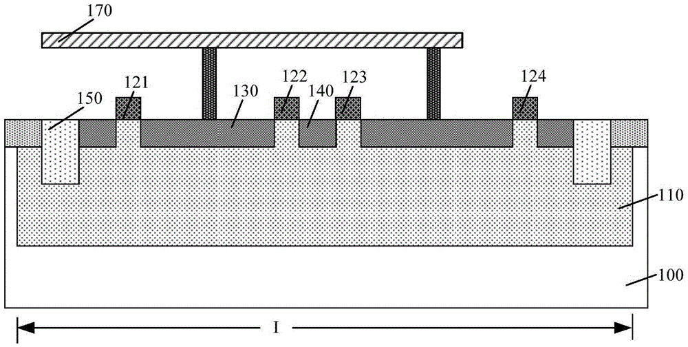
[0021] like figure 1 As shown, the structure of an embodiment of GGNMOS includes: a substrate 100; a P-type well region 110 located in the substrate 100, an isolation structure 150 located in the P-type well region 110, and an isolation structure 150 located between the isolation structures 150. The plurality of gate structures on the substrate 100 are located in the N-type doped regions between the gate structures or between the gate structures and the isolation structure 150, and the N-type doped regions are located in the P-type well region 110 .
[0022] Specifically, the plurality of gate structures include a first gate structure 121 , a second gate structure 122 , a third gate structure 123 and a fourth gate structure 124 sequentially located between the isolation structures 150 . The N-type doped region between the fi...
PUM
 Abstract
Description
Claims
Application Information