Circuit board combination and assembly method thereof

An assembly method and circuit board technology, which are applied to circuits, coupling devices, printed circuit components, etc., can solve the problems of different connector specifications of circuit sub-boards, complicated manufacturing processes, and increased production costs, so as to reduce the manufacturing process. Time, simple manufacturing process, and the effect of strengthening the overall structural strength

Inactive Publication Date: 2016-07-20
DELTA ELECTRONICS INC
View PDF5 Cites 4 Cited by
  • Summary
  • Abstract
  • Description
  • Claims
  • Application Information

AI Technical Summary

Problems solved by technology

[0007] An object of the present invention is to provide a circuit board combination to improve the need for additional fixtures to assist and support the circuit sub-board in the prior art, resulting in complicated manufacturing processes, increased production costs, and connector specifications of the circuit sub-board Inconsistent, leading to problems such as poor scalability

Method used


Image

  • Circuit board combination and assembly method thereof
  • Circuit board combination and assembly method thereof
  • Circuit board combination and assembly method thereof

Examples


Embodiment Construction

[0049] Some typical embodiments embodying the features and advantages of the present invention will be described in detail in the description in the following paragraphs. It should be understood that the present invention can have various changes in different embodiments, but none of them departs from the scope of the present invention, and the description and drawings therein are used as illustrations in nature, not to limit the present invention. invention.

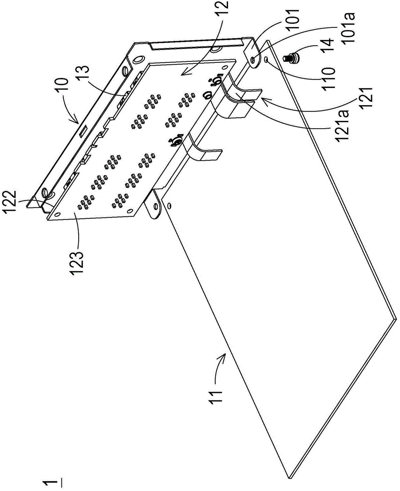
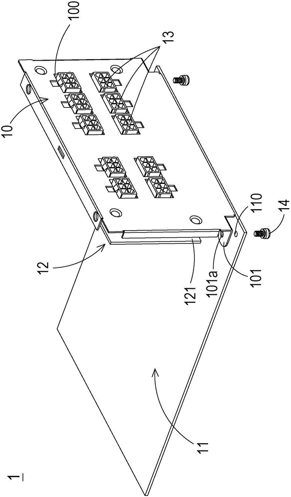
[0050] Please also see Figure 1A and Figure 1B , Figure 1A and Figure 1BThey are respectively the structural schematic diagram of the circuit board assembly and the rear structural schematic diagram of the first preferred embodiment of the present invention. As shown in the figure, the circuit board assembly 1 of the present invention is suitable for use in an electronic device (not shown), and the circuit board assembly 1 consists of a housing 10, a first circuit board 11, a second circuit board 12, a plurality o...


PUM


Abstract

The invention discloses a circuit board combination and an assembly method thereof. The circuit board combination comprises a shell, a first circuit board, a second circuit board and a locking element, wherein the shell comprises a plurality of openings and a first locking part; the first circuit board comprises a second locking part; the second circuit board comprises a docking part; a plurality of connectors are electrically connected with the second circuit board and are arranged through the plurality of openings of the shell, so that the second circuit board is connected with the shell through the plurality of connectors and the second circuit board and the shell are arranged in parallel; and the docking part of the second circuit board is electrically connected with the first circuit board, so that the second circuit board is arranged vertically to the first circuit board, and the first locking part of the shell is connected and locked corresponding to the second locking part of the first circuit board through the locking element. Application of the circuit board combination is relatively wide; the shell is relatively simply and conveniently connected and fixed to the first circuit board and the second circuit board; the manufacturing process time can be shortened; the production cost is reduced; and the overall structural strength of the circuit board combination can be strengthened.

Description

technical field [0001] The invention relates to a circuit board combination, in particular to a circuit board combination using the housing of the electronic device as an auxiliary support structure and an assembly method thereof. Background technique [0002] With the development of the electronics industry, electronic products gradually tend to develop in the direction of modularization. Although electronics companies in different fields carry out production and R&D in their own professional technical fields, as the complex functions of electronic products become increasingly large, terminal Various modules can be combined on electronic products to provide consumers with more integrated and multi-functional electronic products. [0003] Generally speaking, these functional modules are usually packaged in the circuit sub-board and assembled to the system circuit board through the circuit sub-board. Traditionally, there are many ways to assemble the circuit sub-board and the...

Claims


Application Information

Patent Timeline
Patent Type & Authority Applications(China)
IPC IPC(8): H05K1/14H05K3/36
CPCH01R12/716H01R12/722H01R12/73H05K1/14
Inventor 陈鸿川姜盛尧林国桦
Owner DELTA ELECTRONICS INC
Why Eureka
Try Eureka