Array substrate, display panel and display device

A technology of array substrate and color resistance, applied in instruments, nonlinear optics, optics, etc., can solve problems such as affecting the normal display of liquid crystal display panels, and achieve the effect of reducing shrinkage

Inactive Publication Date: 2016-11-16
SHANGHAI AVIC OPTOELECTRONICS +1
View PDF3 Cites 2 Cited by
  • Summary
  • Abstract
  • Description
  • Claims
  • Application Information

AI Technical Summary

Problems solved by technology

[0004] In view of this, the present invention provides an array substrate, a display panel and a display device to solve the problem in the prior art that the normal display of the liquid crystal display panel is affected due to shrinkage of the color resistance

Method used


Image

  • Array substrate, display panel and display device
  • Array substrate, display panel and display device
  • Array substrate, display panel and display device

Examples


Embodiment Construction

[0030] The following will clearly and completely describe the technical solutions in the embodiments of the present invention with reference to the accompanying drawings in the embodiments of the present invention. Obviously, the described embodiments are only some of the embodiments of the present invention, not all of them. Based on the embodiments of the present invention, all other embodiments obtained by persons of ordinary skill in the art without making creative efforts belong to the protection scope of the present invention.

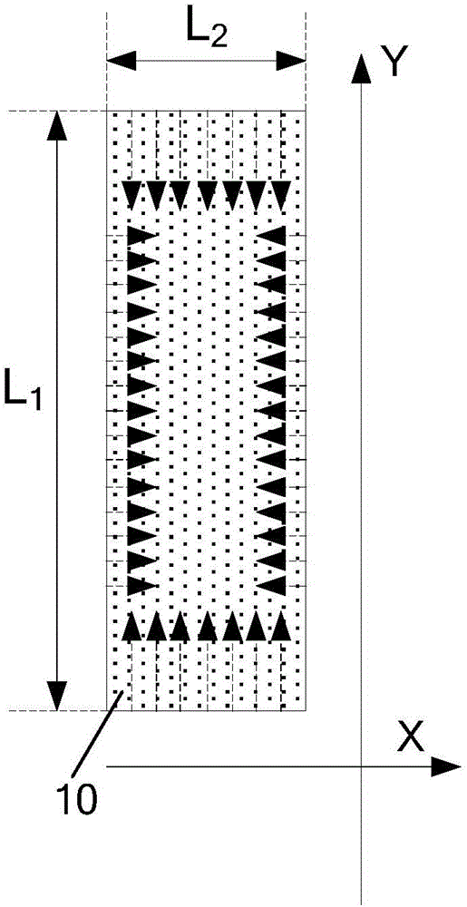
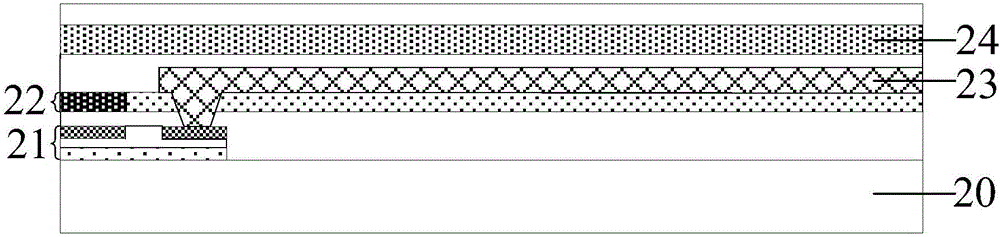
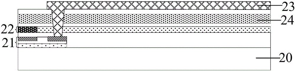
[0031] An embodiment of the present invention provides an array substrate, referring to figure 2 , figure 2 A schematic cross-sectional structure diagram of an array substrate provided by an embodiment of the present invention, the array substrate includes a first substrate 20 and a thin film transistor layer 21 disposed on the surface of the first substrate 20, a color resistance layer 22, a pixel electrode layer 23 and a common electrode Lay...


PUM


Abstract

The invention provides an array substrate, a display panel and a display device. The array substrate comprises a plurality of gate lines and a plurality of data lines, wherein the multiple gate lines and the multiple data lines are crossed in an insulating manner to define a plurality of subpixels; the array substrate further comprises a color resistor layer; the color resistor layer comprises a plurality of color resistors corresponding to at least one subpixel; the length of each color resistor in a first direction is greater than that of the color resistor in a second direction; at least one side edge of each color resistor in the first direction is a curve or a broken line; the first direction is a direction where the gate lines or the data lines extend, and is perpendicular to the second direction. At least one side edge of each color resistor in the first direction is the curve or the broken line, and the stress transmission of the color resistors corresponding to the curve or the broken line in the first direction is broken, so that the shrinkage of the color resistors in the first direction can be reduced, and the influence on normal displaying of a liquid crystal display panel due to the shrinkage of the color resistors is avoided.

Description

technical field [0001] The present invention relates to the technical field of display devices, and more specifically, to an array substrate, a display panel and a display device. Background technique [0002] The prior art discloses a liquid crystal display panel, which includes a color filter substrate, an array substrate, and a liquid crystal layer located between the color filter substrate and the array substrate. The array substrate includes a plurality of gate lines, a plurality of data lines in the display area, and a plurality of sub-pixels defined by insulating intersections of the plurality of gate lines and the plurality of data lines, and each sub-pixel includes a thin film transistor and a pixel electrode. The array substrate also includes a plurality of color resists located in the display area, and each color resist is set corresponding to a plurality of sub-pixels. Moreover, the film layer where the color resistance is located is located between the film lay...

Claims


Application Information

Patent Timeline
IPC IPC(8): G02F1/1362
CPCG02F1/136209G02F1/136286
Inventor 金慧俊
Owner SHANGHAI AVIC OPTOELECTRONICS
Why Eureka
Try Eureka