Pixel circuit and driving method thereof, and display panel

A pixel circuit and circuit technology, applied in static indicators, instruments, etc., can solve the problems of different OLED currents, inability to adjust resolution, uneven threshold voltage of driving thin film transistors, etc., and achieve the effect of avoiding inconsistency

Active Publication Date: 2017-03-15
BOE TECH GRP CO LTD
View PDF10 Cites 24 Cited by
  • Summary
  • Abstract
  • Description
  • Claims
  • Application Information

AI Technical Summary

Problems solved by technology

However, due to the manufacturing process and device aging, in the existing pixel driving circuit, there is non-uniformity in the threshold voltage of the driving thin film transistor driving the light-emitting diode at each pixel point, which leads to the fact that even if the gate of each driving thin film transistor The same driving voltage is applied to each pole, and the current flowing through each OLED may also be different, thus affecting the display effect
[0003] In addition, when the current display screen displays images, the resolution of each area is the same, and it is impossible to dynamically adjust the resolution of a local area of ​​the display screen in real time according to the user's visual focus.

Method used


Image

  • Pixel circuit and driving method thereof, and display panel
  • Pixel circuit and driving method thereof, and display panel
  • Pixel circuit and driving method thereof, and display panel

Examples


Embodiment Construction

[0026] The embodiments of the present disclosure will be clearly and completely described below in conjunction with the accompanying drawings. Apparently, the described embodiments are only some of the embodiments of the present invention, rather than all the embodiments. Based on the embodiments in the present disclosure, all other embodiments obtained by persons of ordinary skill in the art without making creative efforts also fall within the protection scope of the present invention.

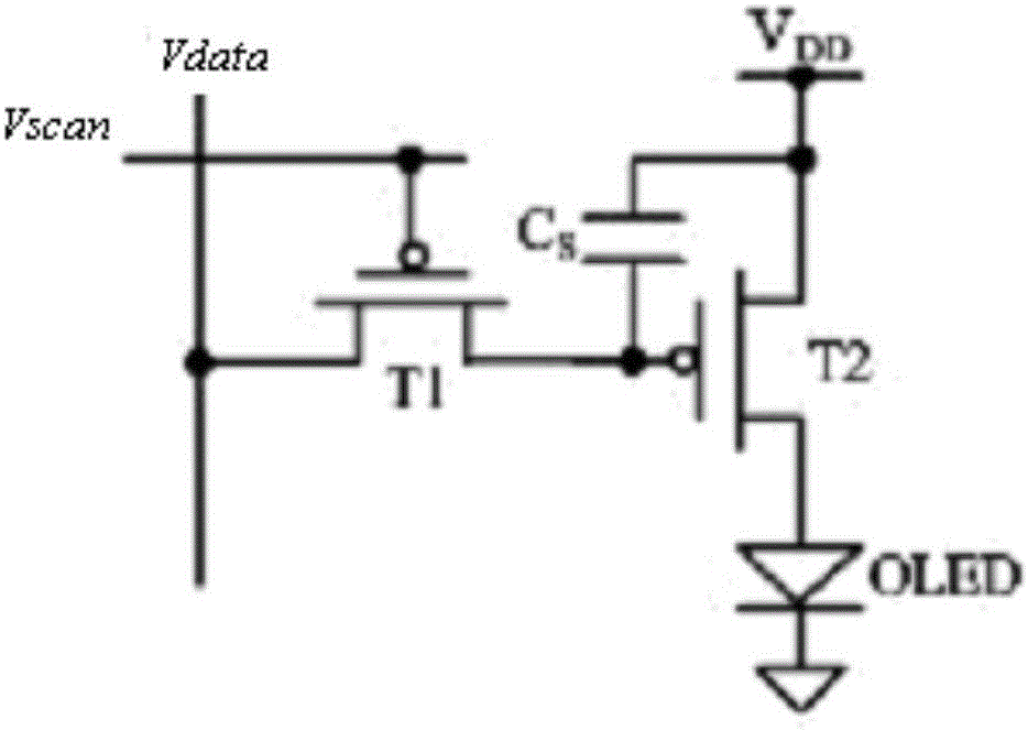
[0027] As mentioned above, there is a threshold voltage of the driving TFT. Due to the process, the threshold voltage Vth of the driving TFT of each pixel may be different; and after a long time of work, the threshold voltage of the driving TFT will also drift, so It will cause uneven brightness of the OLED of each pixel, which will affect the uniformity of display.

[0028] For example, figure 1 A known 2T1C pixel circuit is shown, which includes a drive TFT T2, a switch TFT T1 and a storag...


PUM


Abstract

The invention discloses a pixel circuit and a driving method thereof, and a display panel. The pixel circuit comprises a first sub-pixel circuit and at least one second sub-pixel circuit, wherein the first sub-pixel circuit writes a first data voltage provided by a first data line under control of a first scanning line and generates a compensation voltage at a first node; the at least one second sub-pixel circuit carries out threshold voltage compensation through using the compensation voltage generated at the first node; and based on a display mode, the at least one second sub-pixel circuit writes a second data voltage provided by a second data line under control of a second scanning line. By using the pixel circuit and the driving method thereof, and the display panel, combination of threshold voltage compensation and intelligent display is performed on a driving transistor of the pixel circuit so that an influence of drifting of a threshold voltage on a driving current of the driving transistors can be eliminated, and visual resolution to each area of the display panel is adjusted in real time aiming at a condition that a user pays attention to different points of a frame displayed by the display panel.

Description

technical field [0001] The present disclosure relates to the field of display technology, and in particular to a pixel circuit, a driving method thereof, and a display panel including the pixel circuit. Background technique [0002] With the rapid development of display technology, display screens using organic light-emitting diodes (Organic Light-Emitting Diode, OLED) are one of the hot spots in the field of flat panel display research. Compared with the existing liquid crystal display, it has the advantages of low energy consumption, self-illumination, wide viewing angle and fast response speed, etc. It is easy to match with the integrated circuit driver, and has a wide range of working temperature adaptability, light and thin volume, and easy to realize flexible display ,with broadly application foreground. Different from thin film transistor liquid crystal display (TFT-LCD) which uses voltage to control the brightness of light-emitting transistors, OLED is driven by cur...

Claims


Application Information

Patent Timeline
Patent Type & Authority Applications(China)
IPC IPC(8): G09G3/3225G09G3/3258
CPCG09G3/3225G09G3/3258G09G2320/06G09G3/3233G09G3/3275G09G2300/0452G09G2300/0814G09G2300/0819G09G2300/0842G09G2300/0861G09G2300/0866G09G2310/0262G09G2320/0686G09G2300/043G09G3/3241G09G3/3291
Inventor 陈小川杨盛际张粲王磊
Owner BOE TECH GRP CO LTD
Why Eureka
Try Eureka