Brightness adjusting method and brightness adjusting system of a kind of oled display panel

A display panel and display brightness technology, applied in static indicators, instruments, etc., can solve problems affecting image display quality, high number of pixels per inch, increase in process difficulty, etc., to achieve uneven luminescence, high brightness adjustment accuracy, The effect of reducing the difficulty of the process

Active Publication Date: 2019-06-11
WUHAN TIANMA MICRO ELECTRONICS CO LTD
View PDF8 Cites 0 Cited by
  • Summary
  • Abstract
  • Description
  • Claims
  • Application Information

AI Technical Summary

Problems solved by technology

[0003] However, in the existing OLED display panel, due to reasons such as manufacturing process and aging of luminescent materials, it is easy to cause uneven light emission between sub-pixels, that is, when sub-pixels of the same color are input with the same image signal, the display brightness is different, which affects the image display quality.
[0004] In the prior art, the method of compensating the driving circuit of the thin-film transistor is usually used to improve the unevenness of light emission. However, this method often requires the design of a more complex pixel circuit, which not only increases the difficulty of the process, but also limits the area of ​​the light-emitting area, making it impossible to achieve more Highest number of pixels per inch (Pixels Per Inch, PPI)

Method used


Image

  • Brightness adjusting method and brightness adjusting system of a kind of oled display panel
  • Brightness adjusting method and brightness adjusting system of a kind of oled display panel
  • Brightness adjusting method and brightness adjusting system of a kind of oled display panel

Examples


Embodiment Construction

[0020] The present invention will be further described in detail below in conjunction with the accompanying drawings and embodiments. It should be understood that the specific embodiments described here are only used to explain the present invention, but not to limit the present invention. In addition, it should be noted that, for the convenience of description, only some structures related to the present invention are shown in the drawings but not all structures.

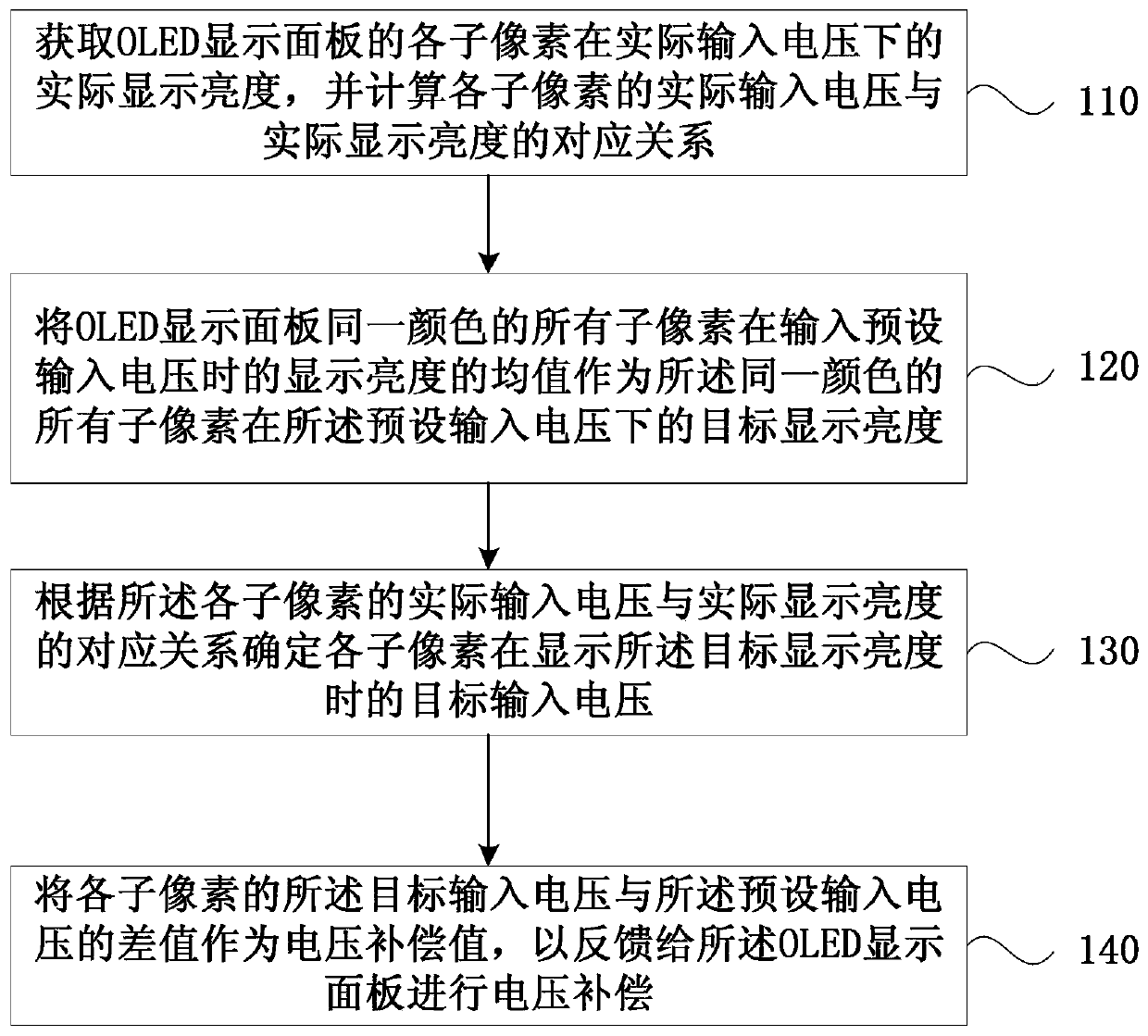
[0021] figure 1 For a flow chart of a brightness adjustment method for an OLED display panel provided in Embodiment 1 of the present invention, refer to figure 1 , the brightness adjustment method may specifically include the following steps:

[0022] Step 110: Acquire the actual display brightness of each sub-pixel of the OLED display panel under the actual input voltage, and calculate the corresponding relationship between the actual input voltage of each sub-pixel and the actual display brightness.

[0023] S...


PUM


Abstract

An embodiment of the invention discloses a brightness adjusting method and system of an OLED display panel. The method includes: acquiring the actual display brightness of each subpixel of the OLED display panel under actual input voltage, and calculating the corresponding relationship between the actual input voltage of each subpixel and the actual display brightness; using the average value of the display brightness of all the same-color subpixels of the OLED display panel under preset input voltage as the target display brightness of all the same-color subpixels of the OLED display panel under the preset input voltage; determining the target input voltage of each subpixel when the subpixel displays the target display brightness according to the corresponding relationship between the actual input voltage of each subpixel and the actual display brightness; using the difference value of the target input voltage of each subpixel and the preset input voltage as the voltage compensation value which is fed back to the OLED display panel for voltage compensation. By the brightness adjusting method, light-emitting unevenness among the subpixels of the OLED display panel is improved.

Description

technical field [0001] Embodiments of the present invention relate to display technology, and in particular, to a brightness adjustment method and a brightness adjustment system of an OLED display panel. Background technique [0002] With the development of display technology, the display effect of display products has been continuously improved, so that the application of display products has become more and more extensive. [0003] However, in the existing OLED display panel, due to reasons such as manufacturing process and aging of luminescent materials, it is easy to cause uneven light emission between sub-pixels, that is, when sub-pixels of the same color are input with the same image signal, the display brightness is different, which affects the image display quality. . [0004] In the prior art, the method of compensating the driving circuit of the thin-film transistor is usually used to improve the unevenness of light emission. However, this method often requires th...

Claims


Application Information

Patent Timeline
Patent Type & Authority Patents(China)
IPC IPC(8): G09G3/3208
CPCG09G3/3208G09G2320/0626
Inventor 边青吕博嘉孔祥梓
Owner WUHAN TIANMA MICRO ELECTRONICS CO LTD
Why Eureka
Try Eureka