Communication circuit and debugging method based on i2c bus

A communication circuit and debugging method technology, applied in the direction of bus network, data exchange through path configuration, electrical components, etc., can solve problems such as I2C address conflicts, reduce production costs, etc., and achieve improved stability, low cost, and simple circuit structure Effect

Active Publication Date: 2021-05-28
GUANGZHOU SHIYUAN ELECTRONICS CO LTD +1
View PDF0 Cites 0 Cited by
  • Summary
  • Abstract
  • Description
  • Claims
  • Application Information

AI Technical Summary

Problems solved by technology

[0005] Based on this, in view of the above problems, the present invention provides a communication circuit and debugging method based on the I2C bus to solve the problem of I2C address conflicts and reduce production costs

Method used


Image

  • Communication circuit and debugging method based on i2c bus
  • Communication circuit and debugging method based on i2c bus
  • Communication circuit and debugging method based on i2c bus

Examples


Embodiment Construction

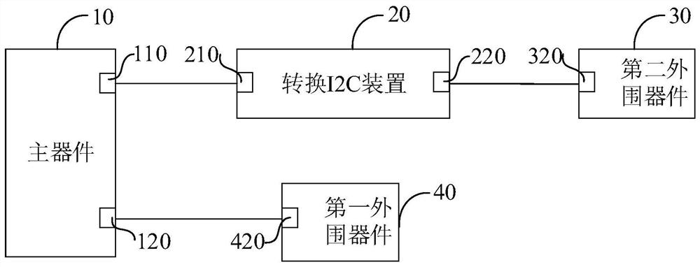
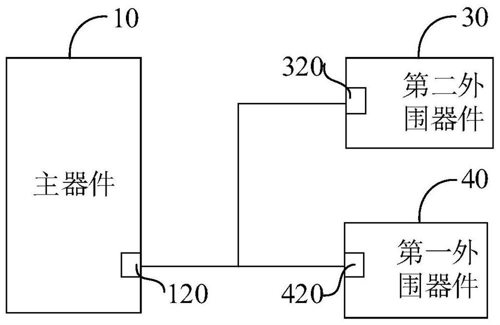
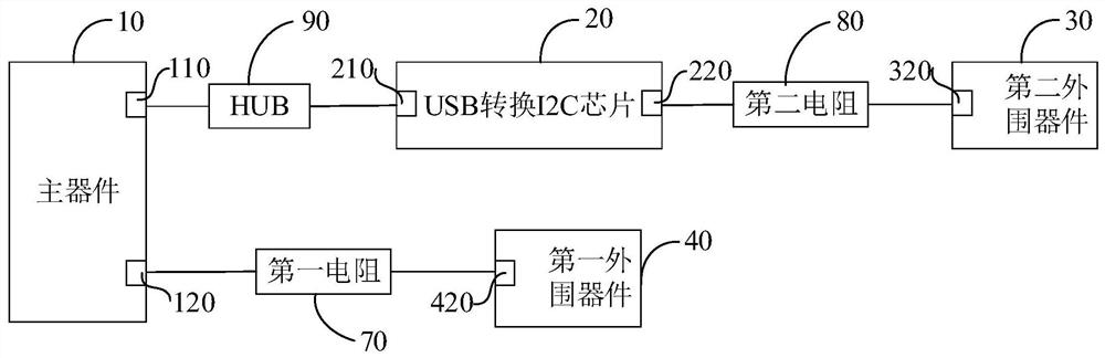
[0030] In order to make the purpose, technical solution and advantages of the present invention clearer, the communication circuit based on the I2C bus of the present invention will be further described in detail below through the embodiments and in conjunction with the accompanying drawings.

[0031] It should be understood that, unless otherwise defined, all technical and scientific terms used herein have the same meaning as commonly understood by those skilled in the technical field of the present invention; the terms "first", "second" and the like are only used for descriptive purposes , but cannot be interpreted as indicating or implying relative importance and knowing the number of technical features indicated by implicit indication; thus, the features defined as "first", "second" and so on may expressly or implicitly include one or more A plurality of such features; in the description of the present invention, unless otherwise specified, "a plurality" means two or more. ...


PUM


Abstract

The invention discloses a communication circuit and a debugging method based on an I2C bus. The circuit includes a master device and a conversion I2C device. Both the master device and the conversion I2C device are provided with an I2C interface and a conversion interface. The I2C interface of the master device is used to connect the A peripheral device, the conversion interface of the main device is connected with the conversion interface of the conversion I2C device, and the I2C interface of the conversion I2C device is used to connect the second peripheral device; when the first peripheral device and the second peripheral device address connected to the same road I2C bus In the event of a conflict, by introducing a conversion I2C device, the non-I2C protocol data and the I2C protocol data are converted to realize bidirectional data transmission between the master device and the second peripheral device, and solve the 12C address conflict between the first peripheral device and the second peripheral device There is no need to adjust conflicting peripheral devices to other 12C buses to improve the stability of software and hardware; at the same time, the circuit structure is simple and the cost is low.

Description

technical field [0001] The invention relates to the field of communication control, in particular to an I2C bus-based communication circuit and a debugging method. Background technique [0002] Modern large-scale communication equipment and electromechanical equipment are connected by many electronic devices through the I2C bus (Inter-Integrated Circuit, internal integrated circuit bus); the I2C bus is a simple, two-way two-wire synchronous serial bus developed by Philips. Only two wires are required to transfer data between devices connected to the bus. [0003] The same I2C bus can connect the main device and multiple peripheral devices. The address of the peripheral device is composed of two parts: the device address and the pin address. fixed and cannot be changed; the pin address is determined by the address pin of the peripheral device on the I2C bus, and different address codes are formed according to the difference between the device connected to the positive pole o...

Claims


Application Information

Patent Timeline
Patent Type & Authority Patents(China)
IPC IPC(8): H04L29/12H04L12/40
CPCH04L12/40078H04L61/5046
Inventor 刘伟
Owner GUANGZHOU SHIYUAN ELECTRONICS CO LTD
Why Eureka
Try Eureka