A display substrate, display panel, touch display device and manufacturing method thereof

A technology of a touch display device and a display panel, which is applied in the fields of display substrates, display panels, and touch display devices, and can solve problems such as the complicated binding process of an external touch display device, and reduce binding steps and simplify binding. The effect of the given process

Active Publication Date: 2020-12-01
BOE TECH GRP CO LTD +1
View PDF5 Cites 0 Cited by
  • Summary
  • Abstract
  • Description
  • Claims
  • Application Information

AI Technical Summary

Problems solved by technology

[0003] In view of this, the present invention provides a display substrate, a display panel, a touch display device and a manufacturing method thereof, which are used to solve the problem of the complicated binding process of the existing plug-in touch display device

Method used


Image

  • A display substrate, display panel, touch display device and manufacturing method thereof
  • A display substrate, display panel, touch display device and manufacturing method thereof
  • A display substrate, display panel, touch display device and manufacturing method thereof

Examples


Embodiment Construction

[0047] In order to make the purpose, technical solutions and advantages of the embodiments of the present invention more clear, the following will clearly and completely describe the technical solutions of the embodiments of the present invention in conjunction with the drawings of the embodiments of the present invention. Apparently, the described embodiments are some, not all, embodiments of the present invention. All other embodiments obtained by those skilled in the art based on the described embodiments of the present invention belong to the protection scope of the present invention.

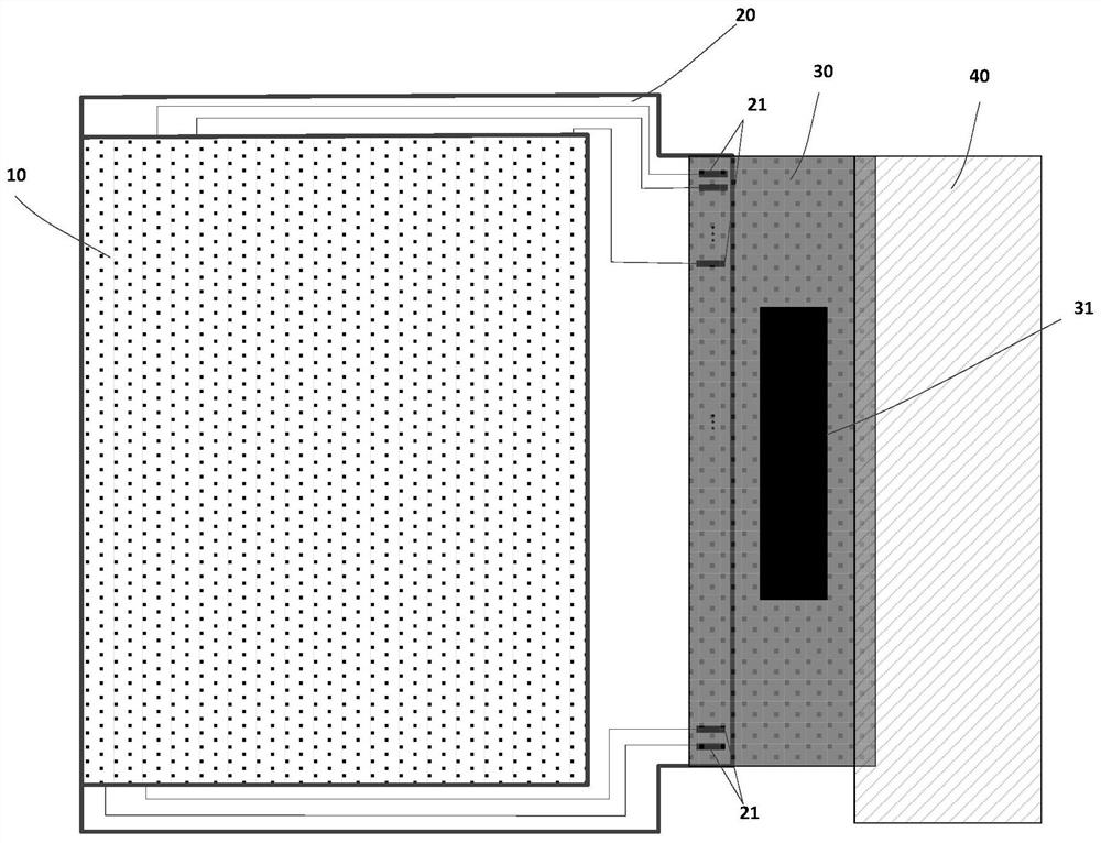
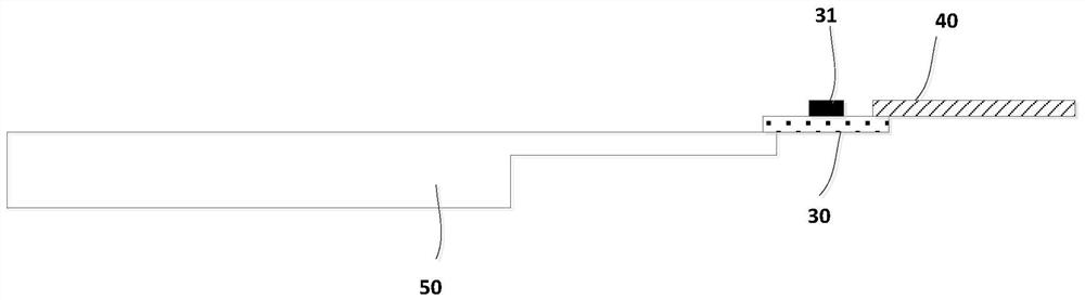
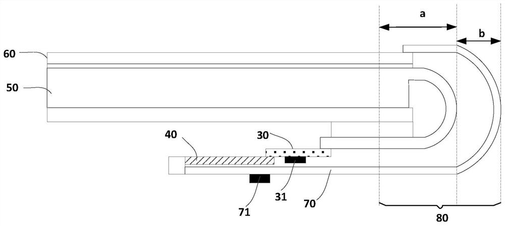
[0048] Please refer to figure 1 , figure 2 with image 3 , figure 1 It is a top view of the binding of the existing display panel with the chip-on-chip film and the main flexible circuit board, figure 2 Side view for existing display panel bonded with COF and main flex circuit board, image 3 It is a side view of an existing touch display device including a display panel and a touch ...


PUM


Abstract

The invention provides a display substrate, a display panel, a touch display device and a manufacturing method thereof. The display substrate includes a display area and a non-display area, and a plurality of first binding pins and a plurality of second binding pins are arranged in the non-display area. Binding pins; the first binding pins are used for binding with the flexible circuit board, and some of the first binding pins are connected to the signal lines set in the display area, so that the signal lines can pass through the first binding pins and connect with the flexible circuit board. The driver integrated circuit on the flexible circuit board is connected; the second binding pin is used for binding with the touch panel, and the second binding pin is connected with another part of the first binding pin in a one-to-one correspondence, so that the touch panel The touch electrodes can communicate with the touch integrated circuit on the flexible circuit board through the second binding pin and the first binding pin. Using the display substrate can reduce the binding steps in the binding process of the touch display device with the display substrate, and can also enable the touch display device with the display substrate to realize an ultra-narrow frame.

Description

technical field [0001] The present invention relates to the field of display technology, in particular to a display substrate, a display panel, a touch display device and a manufacturing method thereof. Background technique [0002] The plug-in touch display device is to stick the plug-in touch screen on the outside of the display panel. In the prior art, when carrying out the bonding (bonding) process of the plug-in touch display device, firstly, it is necessary to connect the display panel to a Chip On Flex (Chip On Flex, or Chip On Flex) film provided with a driver IC (Driver IC). On Film (referred to as COF) and the main flexible circuit board (Main Flexible Printed Circuit, referred to as MFPC) binding, the touch panel and the touch flexible circuit board (Touch Flexible Printed Circuit) equipped with a touch integrated circuit (Touch IC), TFPC for short), then attach the touch panel to the display panel, and finally, bind the main flexible circuit board to the touch f...

Claims


Application Information

Patent Timeline
Patent Type & Authority Patents(China)
IPC IPC(8): G06F3/041
CPCG06F3/0412G06F2203/04103G06F2203/04102G02F1/13338G02F1/13452H05K1/147H05K2201/10136H05K2201/10128H05K2201/09409H10K59/40G02F1/133528G02F1/136286H05K1/028H05K1/189H10K50/87H10K50/868H10K59/131H10K71/00
Inventor 罗鸿强吴建君张光均赵海瑞
Owner BOE TECH GRP CO LTD
Why Eureka
Try Eureka