Touch display panel, manufacturing method thereof and touch display device

A technology for a touch display panel and a manufacturing method, which are applied in the fields of instruments, electrical digital data processing, and data processing input/output processes, etc., can solve the development direction that is not suitable for the thinning of products, the interference of TFT scanning signals, and the overall thickness of the product. Thickness and other problems, to achieve the effect of flexible display touch, enhance stability and sensitivity, and reduce interference

Active Publication Date: 2019-04-23
WUHAN CHINA STAR OPTOELECTRONICS SEMICON DISPLAY TECH CO LTD
View PDF7 Cites 17 Cited by
  • Summary
  • Abstract
  • Description
  • Claims
  • Application Information

AI Technical Summary

Problems solved by technology

Since this structure is only suitable for making rigid AMOLED displays, and the overall thickness of the product is relatively thick, it is not suitable for the current development direction of thinner and lighter products.
[0004] In addition, when the touch sensing circuit is made on the (Thin Film Encapsulation; TFE) thin film encapsulation layer of the AMOLED display, since the touch sensor (touch sensor) is very close to the TFT layer, it is very easy to be interfered by the TFT scanning signal, such as generating Signal interference such as noise (noise) causes the touch function to fail to work normally and effectively

Method used


Image

  • Touch display panel, manufacturing method thereof and touch display device
  • Touch display panel, manufacturing method thereof and touch display device
  • Touch display panel, manufacturing method thereof and touch display device

Examples


Embodiment Construction

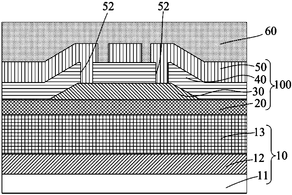
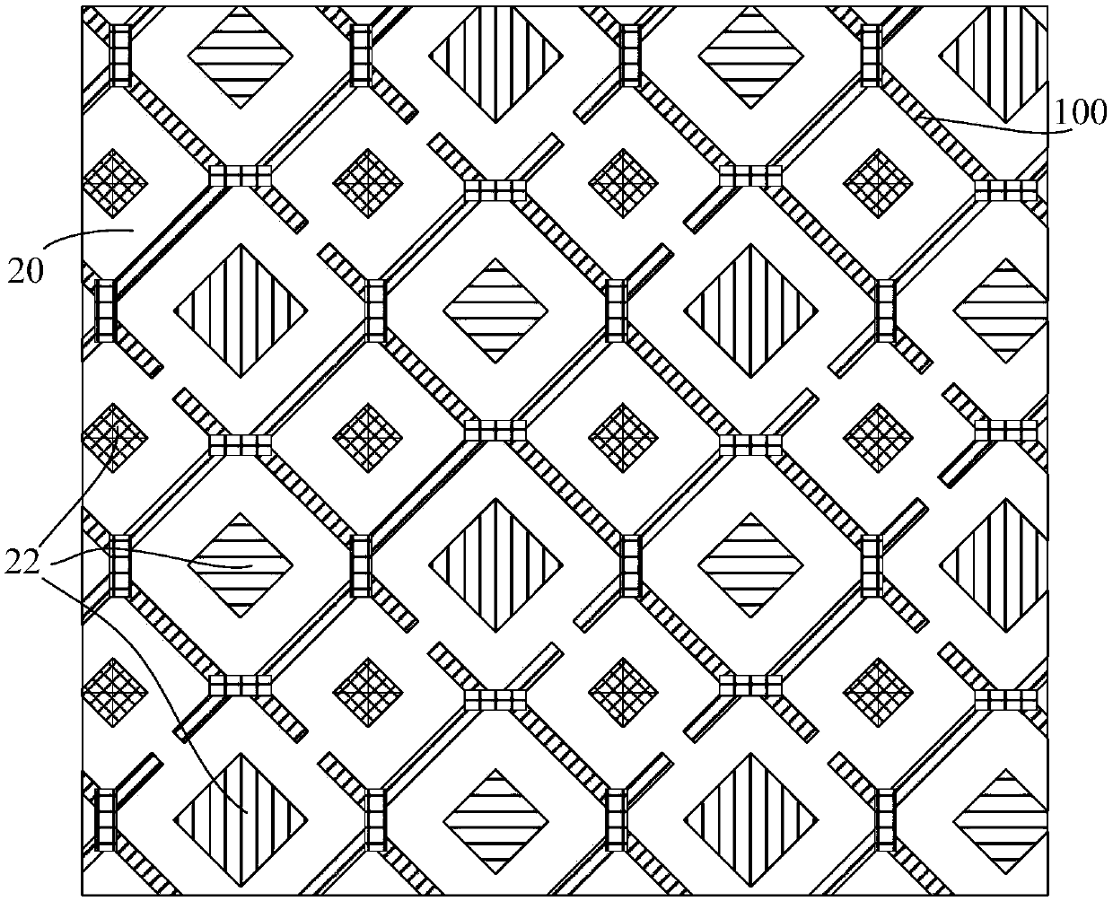
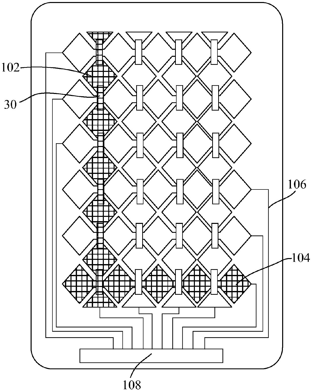
[0037] Reference in the detailed description to "an embodiment" means that a particular feature, structure, or characteristic described in connection with the embodiment can be included in at least one embodiment of the invention. The same terms appearing in different positions in the specification are not necessarily limited to the same implementation, but should be understood as independent or alternative implementations from other embodiments. Inspired by the technical solutions disclosed in the embodiments provided in the present invention, those skilled in the art should understand that the embodiments described in the present invention may have other combinations or changes of technical solutions consistent with the concept of the present invention.

[0038] The following descriptions of the various embodiments refer to the accompanying drawings to illustrate specific embodiments in which the present invention can be practiced. The directional terms mentioned in the pres...


PUM


Abstract

The invention provides a touch display panel, a manufacturing method thereof and a touch display device. The touch display panel comprises a flexible substrate and a metal grid touch electrode layer.The metal grid touch electrode layer is arranged on the flexible substrate, and the metal grid touch electrode layer is provided with a plurality of driving electrodes and a plurality of sensing electrodes. A plurality of floating electrodes are arranged in each driving electrode and each sensing electrode at intervals, the floating electrodes are insulated from the driving electrodes and the sensing electrodes, and the floating electrodes, the driving electrodes and the sensing electrodes are arranged on the same layer. Therefore, the interference signal of the OLED layer is shielded and dispersed, so that the touch sensitivity is improved.

Description

technical field [0001] The present invention relates to the field of display technology, in particular to a touch display panel, a manufacturing method thereof, and a touch display device. Background technique [0002] In recent years, the active matrix organic light emitting diode (Active Matrix Organic Light Emitting Diode; AMOLED) display technology has developed rapidly, and the corresponding touch control scheme has also been followed up simultaneously. Currently, the touch technologies used with AMOLED displays mainly include add-on type (Add on Type) touch film bonding technology and glass encapsulation (On-Cell) technology. Whether it is the plug-in or glass packaging technology, there is a problem of increasing the thickness of the product and affecting the design of the narrow frame. [0003] The external touch film lamination technology uses optical clear adhesive (Optical Clear Adhesive; OCA) to bond the touch film and the AMOLED display together. Depending on ...

Claims


Application Information

Patent Timeline
Patent Type & Authority Applications(China)
IPC IPC(8): G06F3/041
CPCG06F3/041
Inventor 李波
Owner WUHAN CHINA STAR OPTOELECTRONICS SEMICON DISPLAY TECH CO LTD
Why Eureka
Try Eureka