Optical device

An optical device and visible light technology, applied in the field of infrared optics, can solve problems such as unsolvable packaging process and complexity of white light compensation, achieve excellent reliability and performance, realize white light compensation, and have good application prospects

Active Publication Date: 2019-11-12
GRIREM ADVANCED MATERIALS CO LTD
View PDF9 Cites 2 Cited by
  • Summary
  • Abstract
  • Description
  • Claims
  • Application Information

AI Technical Summary

Problems solved by technology

At present, the main problem of this implementation method is that this implementation method still cannot

Method used


Image

  • Optical device
  • Optical device
  • Optical device

Examples


Embodiment 1

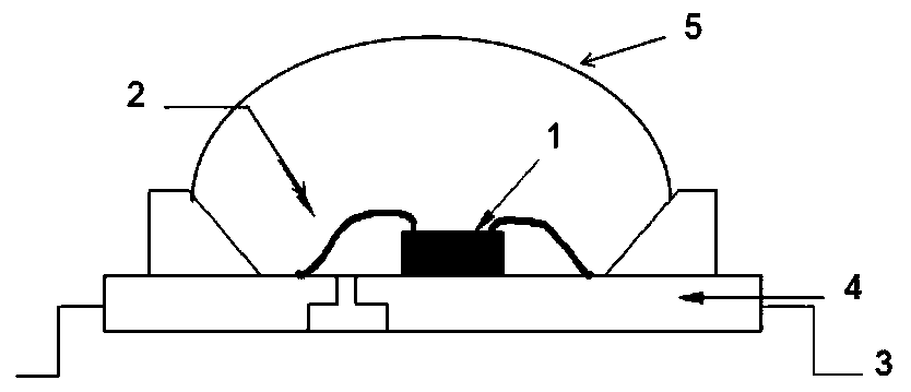
[0042] An optical device, the components of which are a blue LED chip with a wavelength of 455nm and a molecular formula of Ga 2 o 3 . 0.05Cr 2 o 3 : Cr 3+ Near-infrared luminescent material, the molecular formula is La 3Si 6 N 11 : Ce 3+ The visible light luminescent material is. The mass ratio of the infrared luminescent material to the visible light luminescent material is 1:1, and the two luminescent materials are uniformly mixed in the silica gel, and the weight ratio of the two luminescent materials in the silica gel is 60%, and then coated on the LED chip, Get a glowing light source.

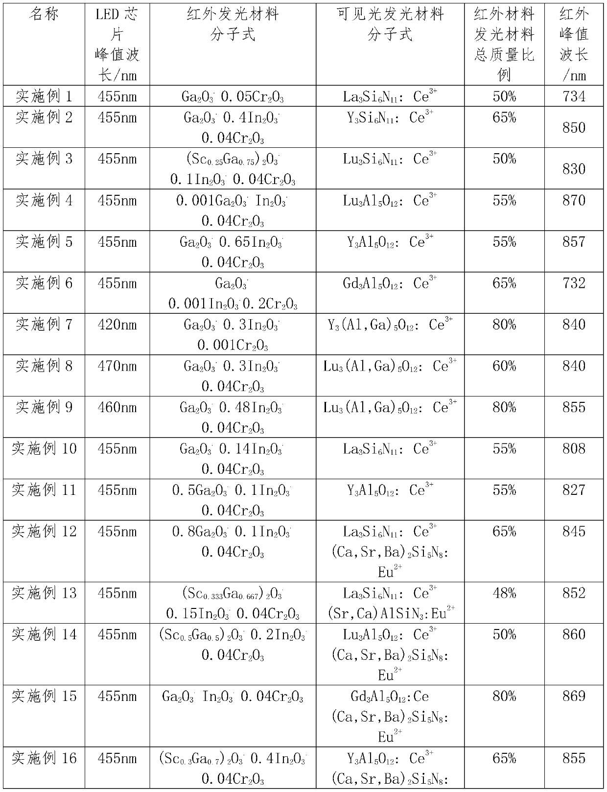
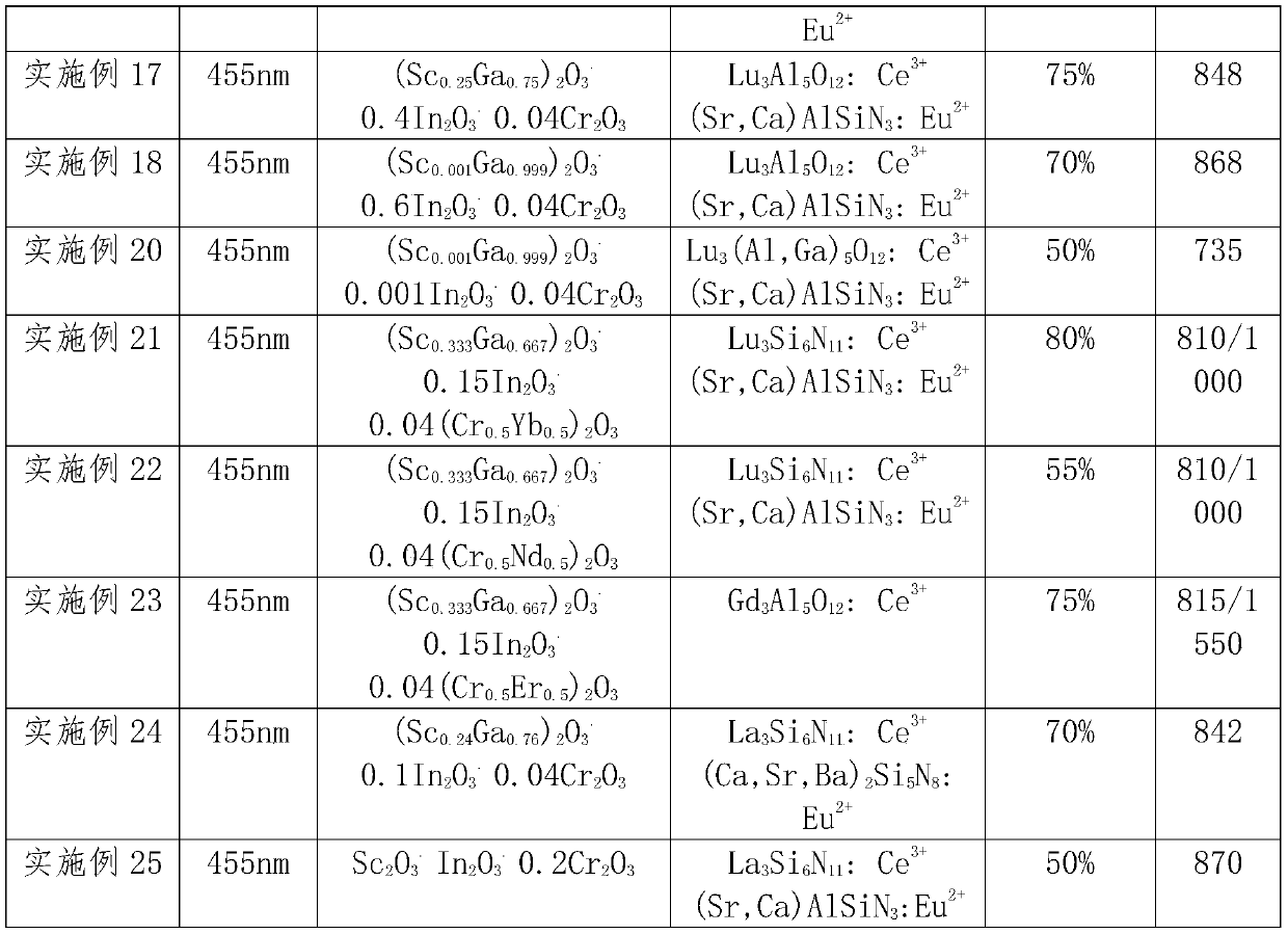
[0043] For the optical devices described in Examples 2-25, the compositions of the luminescent materials are listed in Table 1 below. The structure of the optical devices in each embodiment is the same as in Example 1, only according to the molecular formula of the luminescent materials in each embodiment, according to The respective ratios are mixed to obtain.

[0044] Table 1...


PUM


Abstract

The invention relates to an optical device. The optical device comprises an LED chip, a Ce<3+> simulated visible light-emitting material and a near-infrared light-emitting material xA<2>O<3>.yIn<2>O<3>.bR<2>O<3> compound, wherein an A element in the near-infrared light-emitting material is Sc and/or Ga element, an R element is one or two of elements of Cr, Yb, Nd or Er, Cr is doubtlessly contained, x is more than or equal to 0.001 but less than or equal to 1, y is more than or equal to 0 but less than or equal to 1, b is more than or equal to 0.001 but less than or equal to 0.2, and b/(x+y) ismore than or equal to 0.001 but less than or equal to 0.2. The near-infrared light-emitting material has a crystal structure same as Beta-Ga2O3. In the optical device, an implementation mode of an LED chip combined with the near-infrared light-emitting material and the visible light-emitting material is utilized, near infrared light emitting and visible light emitting are simultaneously achievedby the same LED chip, the package process is greatly simplified, the package cost is reduced, the optical device has the characteristics of high light-emitting efficiency, excellent reliability, highinterference resistance and the like, and white-light compensation can be achieved. The optical device provided by the embodiment of the invention has great application prospect in the field of security and protection.

Description

technical field [0001] Embodiments of the present invention relate to the field of infrared optics technology, in particular to LED chip composite near-infrared luminescent materials, Ce 3+ Optical devices activated by visible light-emitting materials. Background technique [0002] In recent years, the application of near-infrared light in the fields of security monitoring, biometrics, 3D sensing, and food / medical testing has become a focus at home and abroad. Among them, near-infrared LEDs have a series of advantages such as good directivity, low power consumption, and small size. has become the focus of international research. At present, the main implementation method of near-infrared LEDs is to use near-infrared semiconductor chips. For example, 850nm and 940nm infrared chips are mainly used in the security field. One or more white LEDs. In this implementation method, the price of infrared chips is relatively high, and multiple chips are packaged at the same time, and...

Claims


Application Information

Patent Timeline
IPC IPC(8): H01L33/50
CPCH01L33/504
Inventor 刘荣辉刘元红陈晓霞马小乐薛原
Owner GRIREM ADVANCED MATERIALS CO LTD
Why Eureka
Try Eureka