Silicon wafer cleaning device and control method thereof

A silicon wafer cleaning and silicon wafer technology, which is used in semiconductor/solid-state device manufacturing, electrical components, circuits, etc., can solve the problems of poor washing effect, small facing angle between silicon wafer and water outlet, etc., and increase the facing angle. , Improve the cleaning effect, improve the effect of flushing area

Active Publication Date: 2020-07-28
XIAN ESWIN MATERIAL TECH CO LTD +1
View PDF17 Cites 5 Cited by
  • Summary
  • Abstract
  • Description
  • Claims
  • Application Information

AI Technical Summary

Problems solved by technology

[0004] The embodiment of the present invention provides a silicon wafer cleaning device and its control method to solve the problem that the angle between the silicon wafer and the water outlet is small during the silicon wafer cleaning process. Issues that result in poor flushing

Method used


Image

  • Silicon wafer cleaning device and control method thereof
  • Silicon wafer cleaning device and control method thereof
  • Silicon wafer cleaning device and control method thereof

Examples


Embodiment Construction

[0029] The following will clearly and completely describe the technical solutions in the embodiments of the present invention with reference to the accompanying drawings in the embodiments of the present invention. Obviously, the described embodiments are some of the embodiments of the present invention, but not all of them. Based on the embodiments of the present invention, all other embodiments obtained by persons of ordinary skill in the art without creative efforts fall within the protection scope of the present invention.

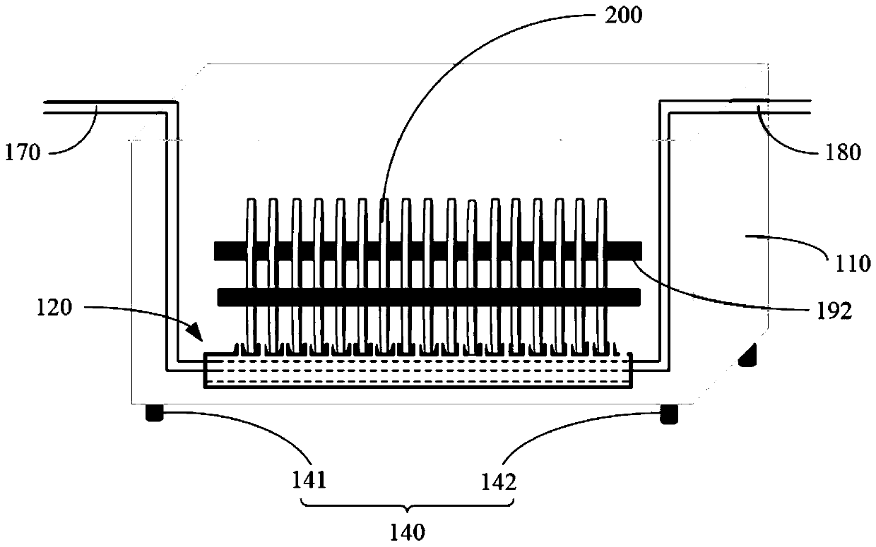
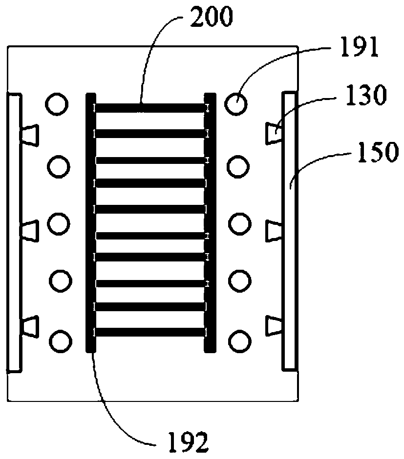
[0030] An embodiment of the present invention provides a silicon wafer cleaning device, such as figure 1 and figure 2 shown, including:

[0031] accommodating tank 110;

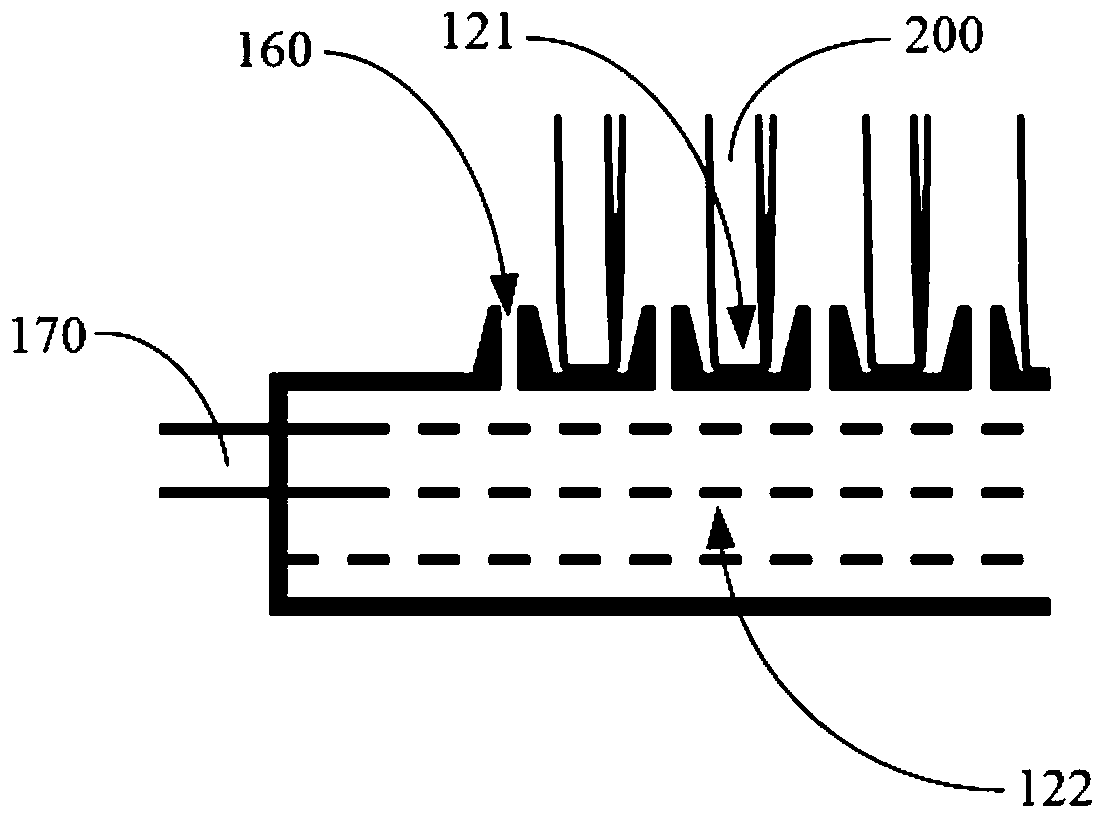
[0032] The bearing seat 120 is located at the bottom wall inside the receiving tank 110 and is used to abut against the silicon chip 200 to carry the silicon chip 200;

[0033] The first water outlet nozzle 130 is located on one side of the opening of the accommodating tank and is...


PUM


Abstract

The invention provides a silicon wafer cleaning device and a control method thereof. The silicon wafer cleaning device comprises a containing groove, a bearing seat which is located on a bottom wall in the containing groove and used for abutting against a silicon wafer so as to bear the silicon wafer, a first water outlet spray head which is located on one side of an opening of the containing groove and faces the silicon wafer, and a lifting assembly, wherein the lifting assembly is connected with the bottom of the containing groove, the lifting assembly comprises a first lifting mechanism located at a first end and a second lifting mechanism located at a second end, the first end and the second end are two opposite ends of the containing groove, and the first lifting mechanism and the second lifting mechanism are used for lifting so as to adjust an inclination angle of the silicon wafer in the containing groove. The silicon wafer cleaning device is advantaged in that the silicon wafercleaning effect can be improved.

Description

technical field [0001] The invention relates to the technical field of silicon wafer processing, in particular to a silicon wafer cleaning device and a control method thereof. Background technique [0002] Single crystal silicon wafers are used as the substrate material of chips. The particles and metals on the surface of silicon wafers have a great impact on the yield of chips. Therefore, it is necessary to use a large amount of pure water to clean the particles on the surface of silicon wafers during the processing of silicon wafers. with metal. [0003] In the related art, the facing angle between the silicon wafer and the water outlet is small during the cleaning process of the silicon wafer, which leads to the problem of poor flushing effect. Contents of the invention [0004] Embodiments of the present invention provide a silicon wafer cleaning device and a control method thereof, so as to solve the problem of poor flushing effect caused by a small direct angle betw...

Claims


Application Information

Patent Timeline
Patent Type & Authority Applications(China)
IPC IPC(8): H01L21/67H01L21/02
CPCH01L21/67051H01L21/02041Y02P70/50
Inventor 曹泽域
Owner XIAN ESWIN MATERIAL TECH CO LTD
Why Eureka
Try Eureka