Circuit board and electronic device

A circuit board and circuit board technology, which is applied to printed circuits, circuit devices, printed circuit components, etc., can solve the problems of circuit board warping and unevenness

Pending Publication Date: 2021-05-18
BOE TECH GRP CO LTD +1
View PDF0 Cites 4 Cited by
  • Summary
  • Abstract
  • Description
  • Claims
  • Application Information

AI Technical Summary

Problems solved by technology

In some technologies, in order to realize the grounding and electromagnetic shielding of the circuit board, it is necessary to open a window on the covering layer covering the circuit layer to expose the grounding circuit of the circuit layer to connect with the electromagnetic interference shielding film or the conductive layer. However, it will cause the circuit board Partial warping, uneven unevenness

Method used


Image

  • Circuit board and electronic device
  • Circuit board and electronic device
  • Circuit board and electronic device

Examples


Embodiment Construction

[0044] The technical solution of the present application will be further described below in conjunction with the accompanying drawings and through specific implementation methods. It should be understood that the specific embodiments described here are only used to explain the present application, but not to limit the present application.

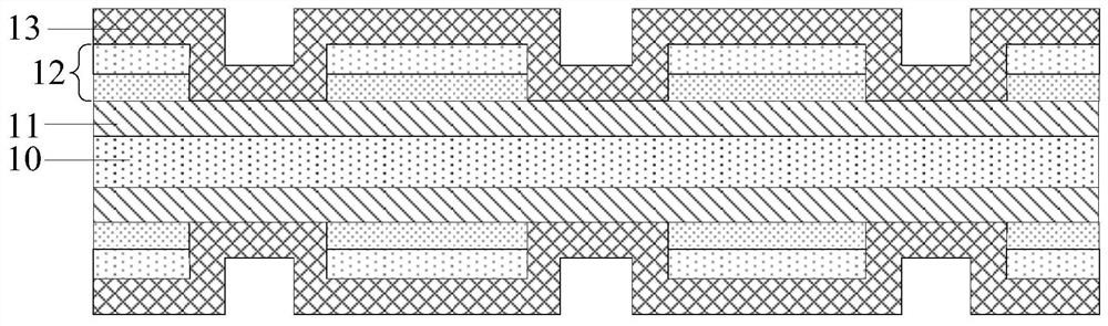
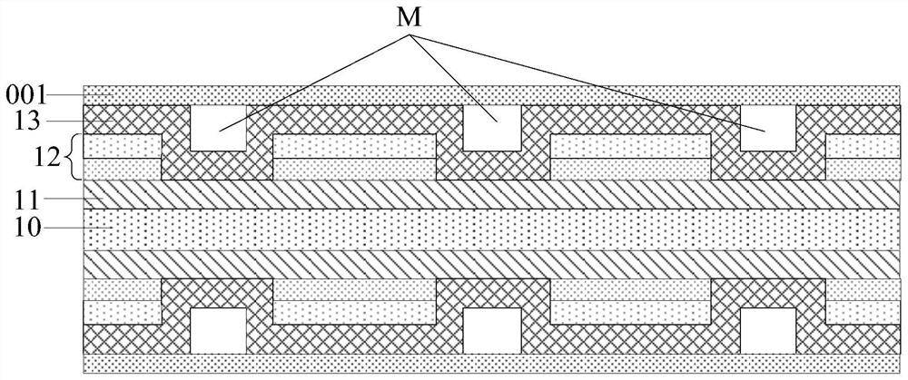
[0045] In some techniques, such as Figure 1a as shown, Figure 1a It is a schematic diagram of the cross-sectional structure of some circuit boards. Because the circuit board needs to have high electromagnetic shielding and signal anti-interference capabilities, an electromagnetic interference shielding film (EMI film for short) 13 will be attached to its surface. (referred to as CVL) 12 to open a window, so that the EMI film 13 is connected to the ground wire of the circuit layer (the circuit layer is arranged on the substrate 10 ) 11 to realize the electromagnetic shielding function of the EMI film 13 . In this grounding method, at the g...


PUM


Abstract

A circuit board and an electronic device relate to but are not limited to the technical field of circuit boards, the circuit board comprises a first circuit board, the first circuit board comprises a first substrate and a first circuit layer arranged on a first side surface of the first substrate, and the first circuit layer comprises a first grounding circuit. The circuit board further comprises a first protection layer and a first electromagnetic interference shielding layer which are sequentially stacked at the side, away from the first substrate, of the first circuit layer. The first protection layer is provided with a first opening, the first opening exposes at least one part of the first grounding line and is filled with a first conductive material, and the height difference between the surface of the first conductive material and the surface, away from the first substrate, of the first protection layer is 0-2 microns. The first conductive material connects the first electromagnetic interference shielding layer and the first ground line. The circuit board provided by the embodiment of the invention can prevent the problems of local upwarp and unevenness after the circuit board is partially windowed to expose the circuit layer.

Description

technical field [0001] Embodiments of the present disclosure relate to but are not limited to the technical field of circuit boards, and specifically relate to a circuit board and electronic equipment. Background technique [0002] At present, electronic products are used more and more widely in daily life, and circuit boards are an important part of electronic products. In some technologies, in order to realize the grounding and electromagnetic shielding of the circuit board, it is necessary to open a window on the covering layer covering the circuit layer to expose the grounding circuit of the circuit layer to connect with the electromagnetic interference shielding film or the conductive layer. However, it will cause the circuit board Partial warping, uneven unevenness. Contents of the invention [0003] The embodiments of the present disclosure provide a circuit board and an electronic device, which can prevent the circuit board from partially warping and unevenness af...

Claims


Application Information

Patent Timeline
Patent Type & Authority Applications(China)
IPC IPC(8): H05K1/02
CPCH05K1/0215H05K1/0219H05K1/028H05K1/0298
Inventor 蒲乾林李飞王梓鉴陆旭
Owner BOE TECH GRP CO LTD
Why Eureka
Try Eureka