

Display device and manufacturing method therefor
A display device and display area technology, which is applied in the manufacture of semiconductor/solid-state devices, electrical components, and electrical solid-state devices, etc., can solve problems such as the reduction of light transmittance in the transmission area, and achieve the effect of preventing the reduction of light transmittance.
- Summary
- Abstract
- Description
- Claims
- Application Information
AI Technical Summary
Problems solved by technology
Method used
Image

Examples
Embodiment Construction
[0041] Hereinafter, a display device and a method of manufacturing the same according to embodiments of the present invention will be described in detail with reference to the accompanying drawings.
[0042] In the following, reference will be made to figure 1 with figure 2 A display device according to an embodiment of the present invention is schematically described.
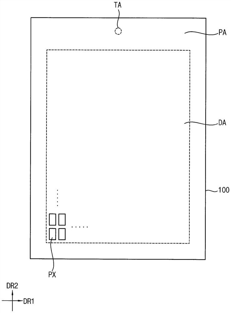
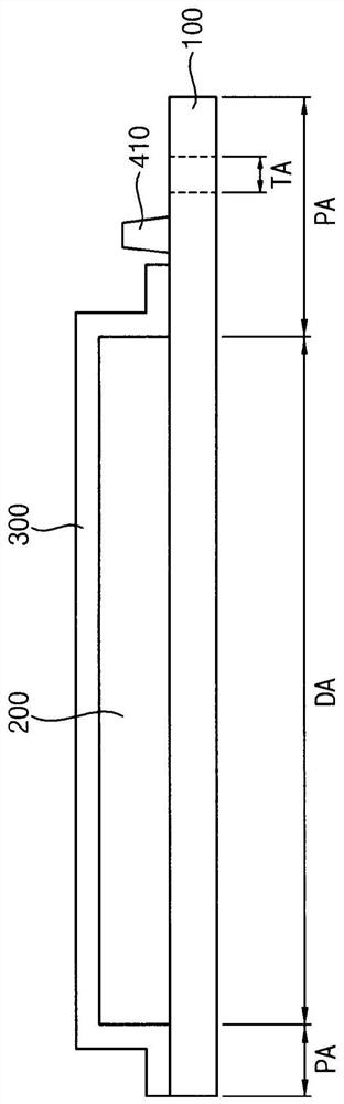
[0043] figure 1 is a plan view showing a display device according to an embodiment of the present invention. figure 2 is schematically shown figure 1 Cutaway view of the display device.
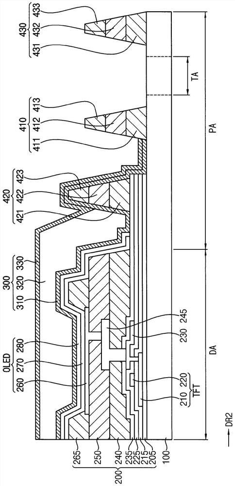
[0044] refer to figure 1 with figure 2 , according to an embodiment of the present invention, a display device may include a substrate 100 , a display unit 200 , a thin film encapsulation layer 300 and a first dam 410 .
[0045] The substrate 100 may include a display area DA and a peripheral area PA. A plurality of pixels PX may be arranged along a first direction DR1 and a second direction DR2 intersecting the fi...
PUM
 Abstract
Description
Claims
Application Information