Circuit board and preparation method thereof

A circuit board and conductive circuit technology, applied in the directions of printed circuit components, electrical connection printed components, and electrical connection formation of printed components, can solve the problems of signal loss, inconsistent cross-sectional size, inconsistent cross-sectional area of ​​vias, etc., to avoid signal Effects of loss and noise

Pending Publication Date: 2022-07-29
HONGQISHENG PRECISION ELECTRONICS (QINHUANGDAO) CO LTD +1
View PDF0 Cites 0 Cited by
  • Summary
  • Abstract
  • Description
  • Claims
  • Application Information

AI Technical Summary

Problems solved by technology

Vias include conductive holes and pads located around the conductive holes, which makes the cross-sectional area of ​​the vias inconsistent; and the size of the vias is limited by drilling and electroplating processes, and the cross-sectional area is often much larger than the cross-section of the conductive lines of each layer Area; As a result, the cross-sectional size of the entire circuit formed by the electrical connection in the circuit board is inconsistent, which will cause signal loss and noise during signal transmission

Method used


Image

  • Circuit board and preparation method thereof
  • Circuit board and preparation method thereof
  • Circuit board and preparation method thereof

Examples


Embodiment Construction

[0047] The technical solutions in the embodiments of the present application will be clearly and completely described below with reference to the drawings in the embodiments of the present application. Obviously, the described embodiments are only a part of the embodiments of the present application, but not all of the embodiments. Based on the embodiments in the present application, all other embodiments obtained by those of ordinary skill in the art without creative efforts fall within the scope of the protection of the present application.

[0048] Unless otherwise defined, all technical and scientific terms used herein have the same meaning as commonly understood by one of ordinary skill in the technical field to which this application belongs. The terms used herein in the specification are for the purpose of describing particular embodiments only and are not intended to limit the application.

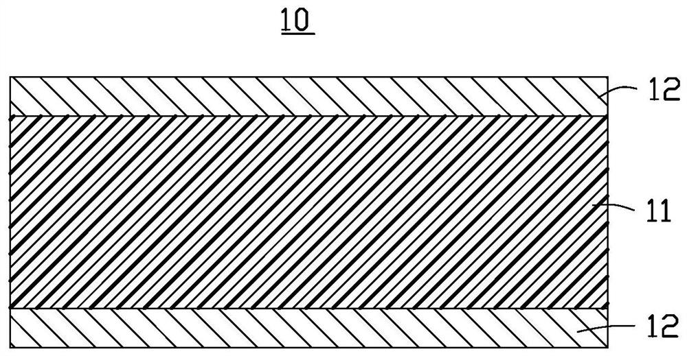
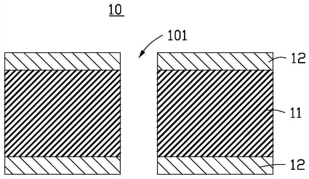
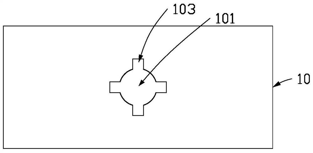
[0049] Please refer to Figure 1 to Figure 13 , the preparation method of the...


PUM


Abstract

The invention provides a preparation method of a circuit board, which comprises the following steps of: providing a substrate, and forming a through hole in the substrate; a groove is formed in the hole wall of the through hole; metalizing the through hole and the groove, so that the hole wall of the through hole is covered with a metal layer; performing circuit manufacturing on the substrate to form two first conductive circuit layers, wherein each first conductive circuit layer comprises a plurality of first conductive circuits; the metal layer covering the hole wall of the through hole is removed to form a first conducting wire, and the first conducting wire and the first conducting circuit which are connected are equal in cross section area. According to the invention, the sectional dimensions of all parts of the whole circuit formed by electrical connection in the circuit board are consistent, so that signal loss and noise can be reduced. The invention further provides a circuit board.

Description

technical field [0001] The present application relates to a circuit board and a preparation method thereof. Background technique [0002] With the trend of miniaturization of electronic devices, the circuit wiring of electronic devices will be denser, and the denser the circuit, the more complicated the circuit wiring will be. If all the circuits are placed on the same layer of circuit board, It is possible that the lines are too close to cause signal interference, so a multi-layer circuit board design is required. [0003] The conductive lines of each layer of the multi-layer circuit board are electrically connected through via holes. Vias include conductive holes and pads around the conductive holes, which makes the cross-sectional area of ​​the vias inconsistent; and the size of the vias is limited by drilling and electroplating processes, and the cross-sectional area is often much larger than the cross-section of the conductive lines of each layer. Therefore, the cross...

Claims


Application Information

Patent Timeline
IPC IPC(8): H05K3/42H05K1/11
CPCH05K3/429H05K1/116H05K2201/09645
Inventor 傅志杰
Owner HONGQISHENG PRECISION ELECTRONICS (QINHUANGDAO) CO LTD
Why Eureka
Try Eureka