Display panel and display device

A technology for display panels and substrates, used in instruments, nonlinear optics, optics, etc., can solve problems such as afterimages and increased charge residues, and achieve the effects of ensuring display effects, improving afterimages, and accelerating ion dissipation.

Pending Publication Date: 2022-08-09
XIAMEN TIANMA MICRO ELECTRONICS
View PDF0 Cites 0 Cited by
  • Summary
  • Abstract
  • Description
  • Claims
  • Application Information

AI Technical Summary

Problems solved by technology

[0003] When the liquid crystal display panel is driven by AC, the positive and negative voltages deviate from the center of symmetry, and the voltage deviated from the center of symmetry is a DC bias voltage, which leads to the directional accumulation of mobile charges in the liquid crystal layer. pole, and further adsorb free ions to generate charges; as the voltage is applied for a longer time, the residual charge generated by the induced polarization inside the alignment film increases. When the voltage is not applied, the residual charge generated by the induced polarization forms a residual DC voltage. As a result, the liquid crystal molecules are not driven by the signal voltage, resulting in afterimages

Method used


Image

  • Display panel and display device
  • Display panel and display device
  • Display panel and display device

Examples


Embodiment Construction

[0029] The embodiments of the present invention will be clearly and completely described below with reference to the accompanying drawings in the embodiments of the present invention. Obviously, the described embodiments are only a part of the embodiments of the present invention, but not all of the embodiments. Based on the embodiments of the present invention, all other embodiments obtained by those of ordinary skill in the art without creative efforts shall fall within the protection scope of the present invention.

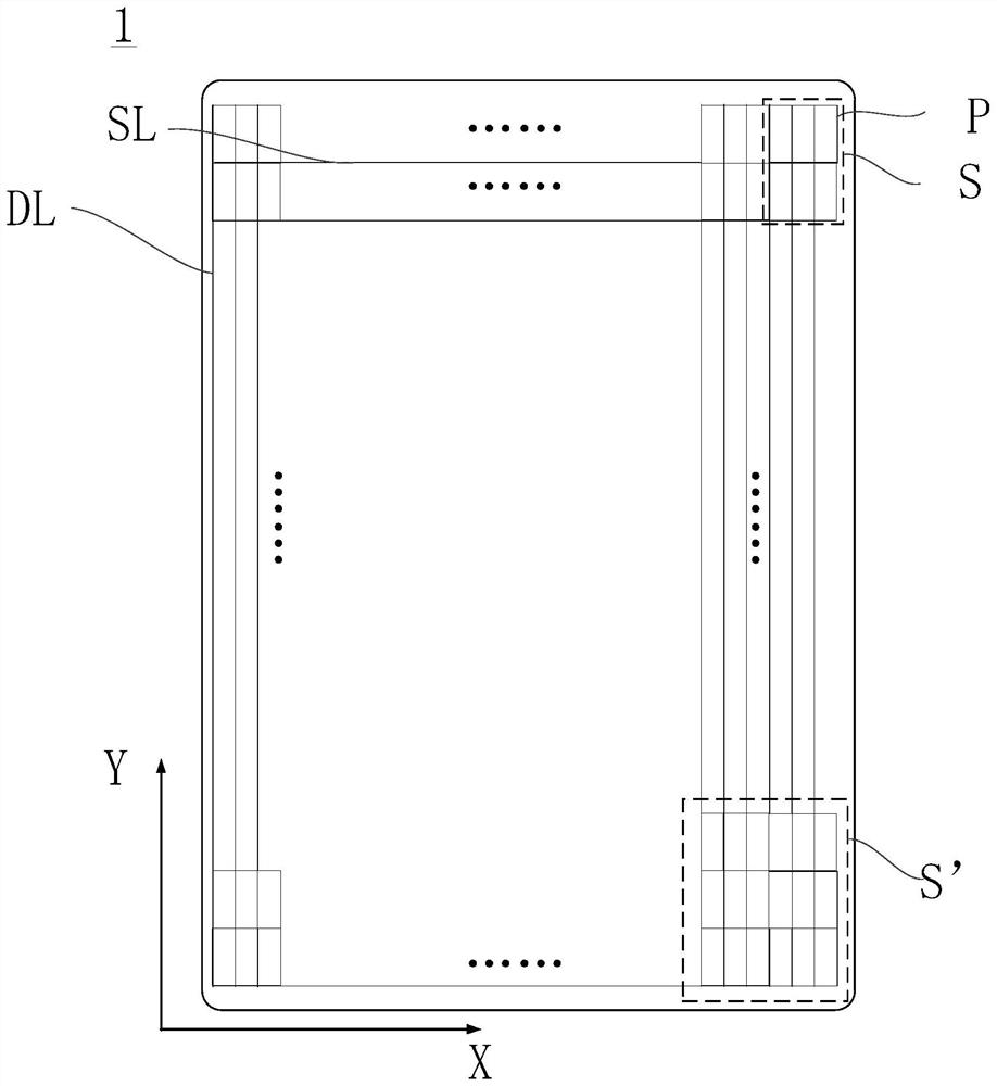
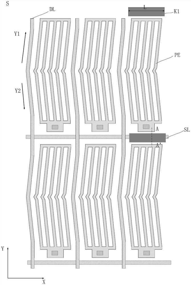
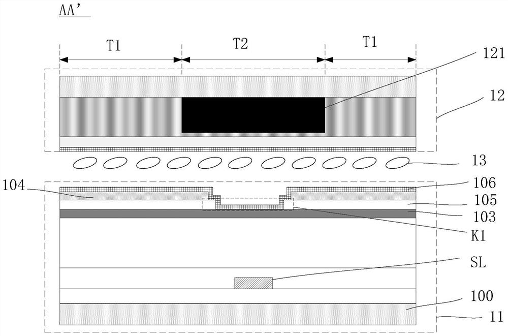
[0030] Please refer to Figure 1 to Figure 3 , figure 1 A schematic top view of a display panel provided by an embodiment of the present invention, figure 2 for figure 1 An enlarged schematic diagram of the S area of ​​the display panel, image 3 for figure 2 A schematic cross-sectional view along the section line AA'; the display panel 1 provided by the embodiment of the present invention includes an array substrate 11, a color filter substrate 12 and a ...


PUM


Abstract

The invention provides a display panel and a display device.The display panel comprises an array substrate, a color film substrate and a liquid crystal layer, the array substrate is sequentially provided with a common electrode layer, a first insulating layer, a pixel electrode layer and an alignment layer, the display panel comprises a plurality of sub-pixel units arranged in an array mode, each sub-pixel unit comprises a pixel electrode, and the pixel electrode is arranged on the first insulating layer. The array substrate comprises a first insulating layer, a plurality of scanning lines extending in the first direction and a plurality of data lines at least partially extending in the second direction, the first direction intersects with the second direction, the first insulating layer is provided with at least one first penetrating part, and in the second direction, the orthographic projection of the first penetrating part on the array substrate is at least located in the area between partial two adjacent pixel electrodes. And in an area corresponding to the first penetrating part, the alignment layer is in contact with the common electrode. According to the invention, the ghosting of the display panel can be improved, and the brightness uniformity of the display panel and the display device can be ensured.

Description

technical field [0001] The present invention relates to the field of display technology, and in particular, to a display panel and a display device. Background technique [0002] Existing liquid crystal display panels include an array substrate, a color filter substrate, and a liquid crystal layer between the array substrate and the color filter substrate. The liquid crystal layer requires alignment films on the array substrate and the color filter substrate for alignment, and the liquid crystal material contains a small amount of ionic impurities, including a small amount of ionic impurities in the liquid crystal layer that may be introduced into the liquid crystal layer in the subsequent preparation process of the liquid crystal panel, such as color resist materials, sealant materials, or in the lamination process of the array substrate and the color filter substrate. pure. [0003] When the liquid crystal display panel is driven by AC, there is a situation where the posi...

Claims


Application Information

Patent Timeline
Patent Type & Authority Applications(China)
IPC IPC(8): G02F1/1335G02F1/1343G02F1/1337
CPCG02F1/133514G02F1/134309G02F1/1337
Inventor 陈建群冯楚慧池明珠方丽婷吴玲
Owner XIAMEN TIANMA MICRO ELECTRONICS
Why Eureka
Try Eureka