

Testing component including work line of memory and capacitor overlaped and offset as well as its testing method
A technology of memory words and test elements, applied in the direction of semiconductor/solid-state device testing/measurement, etc., can solve the problems such as the decrease of the qualification rate of the manufacturing process, the invalidation of the memory cells, and the influence of the size of the doping area.
- Summary
- Abstract
- Description
- Claims
- Application Information
AI Technical Summary
Problems solved by technology
Method used
Image

Examples
Embodiment Construction
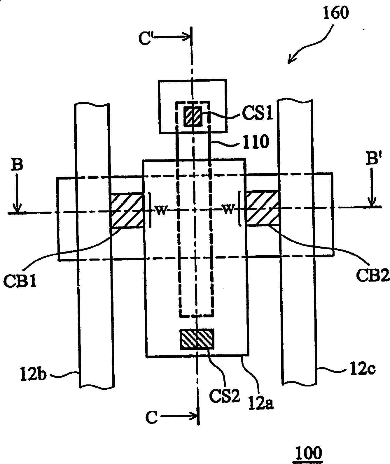
[0016] Please refer to image 3 as well as Figure 4a , Figure 4b , to illustrate an embodiment of the present invention. in image 3 It is a layout diagram of test elements used to detect the overlapping offset of word line structure and deep trench capacitors of a dynamic random access memory in the present invention, wherein the test elements are arranged in the dicing lanes of the chip. Figure 4a it's for image 3 section along the line segment B-B', while Figure 4b it's for image 3 Sectional view along line segment C-C'.
[0017] First, a trench capacitor 110 is disposed on the scribe line region 160 of a chip 100 . The trench capacitor 110 includes a storage node 116, a buried plate 181 in the buried n-type well region NW, and a capacitor dielectric layer therebetween. The storage node 116 is electrically isolated from the doped p-type well region PW by a dielectric collar 126 .
[0018] Next, on the scribe area 160, a rectangular word line 12a, a first pass...
PUM
 Abstract
Description
Claims
Application Information