

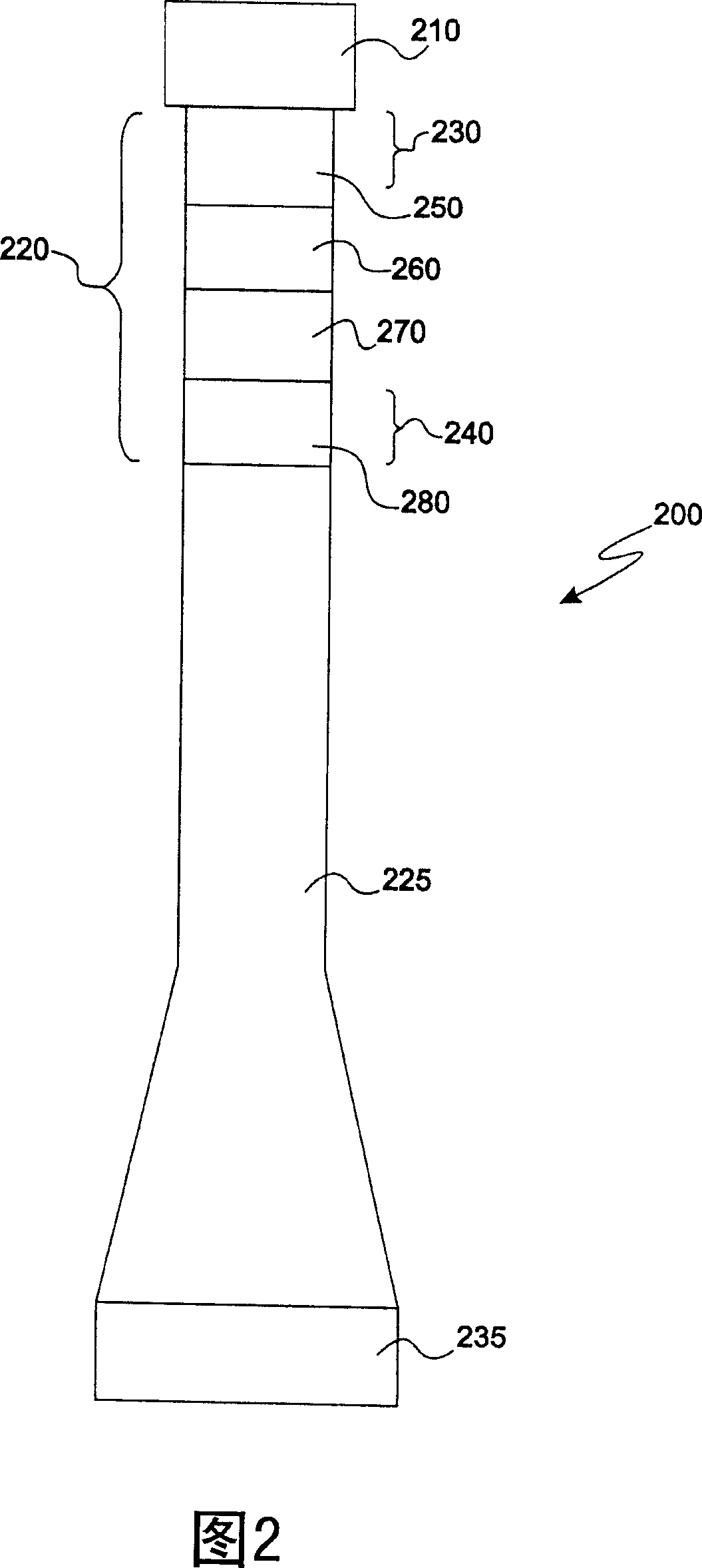
Electron beam accelerator and ceramic stage with electrically-conductive layer or coating therefor
A technology of electron beams and accelerators, applied in the field of electron beam accelerators, can solve the problems of increasing the manufacturing cost of the accelerator 220, and achieve the effects of improving physical strength, reducing costs, and reducing manufacturing costs
- Summary
- Abstract
- Description
- Claims
- Application Information
AI Technical Summary
Problems solved by technology
Method used
Image

Examples
Embodiment Construction
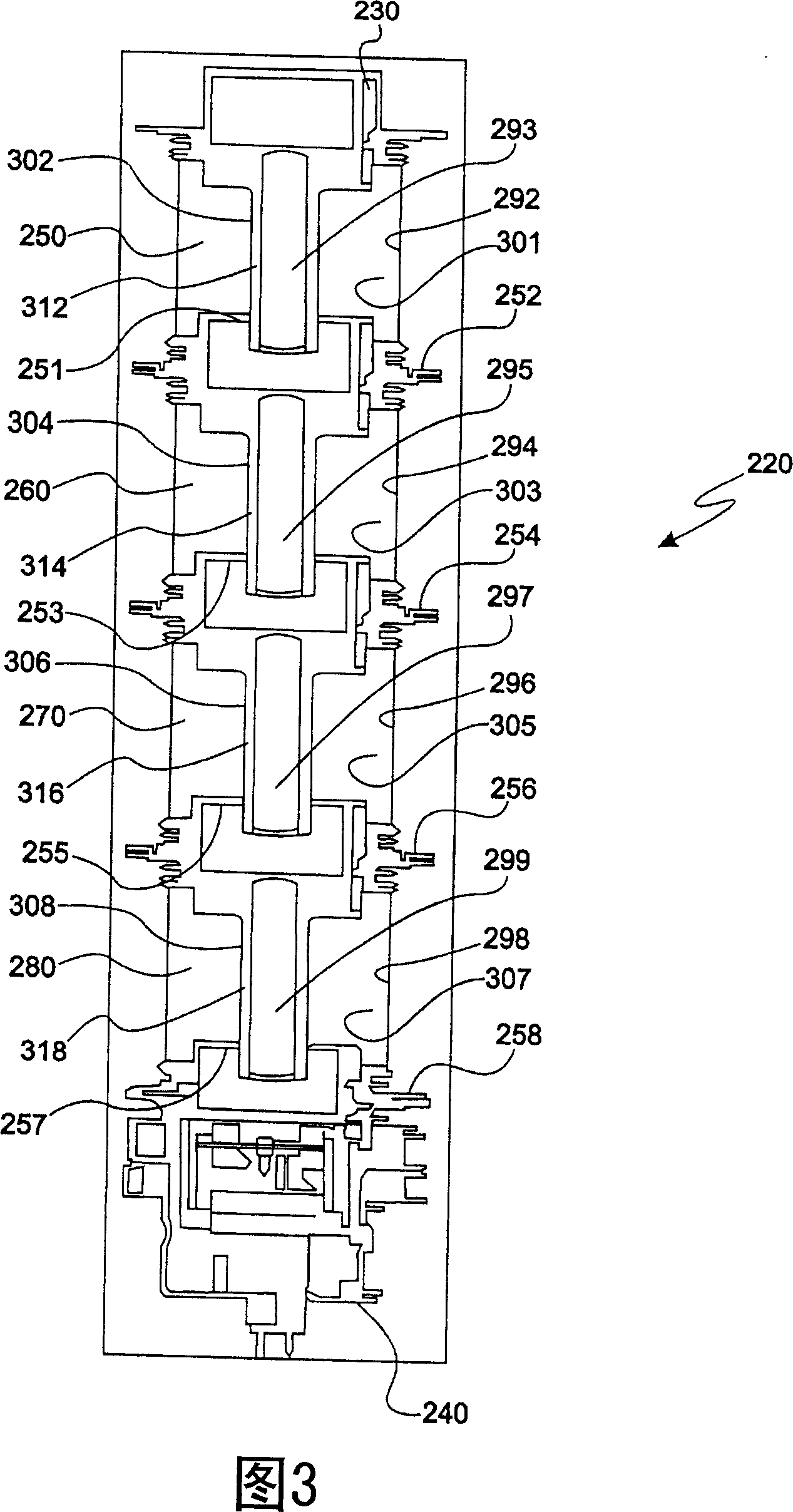
[0025] As used in the specification and claims, the term "ceramic" is meant to include one of the various forms of alumina (particularly Al 2 O3) materials or compositions. The term "layer or coating" includes layers or coatings that are mechanically, chemically, electrically or electrochemically attached to the interior surface of a ceramic body. The term "sleeve" includes within its scope a sleeve or liner that is mechanically, chemically or electrochemically attached to the inner surface of a ceramic body.
[0026] Figure 4A shows a top perspective view of one embodiment of a ceramic body 292 of the present invention. FIG. 4B shows a side view of the ceramic body 292 shown in FIG. 4A. FIG. 4C shows a cross-sectional view of the ceramic body 292 shown in FIG. 4A. FIG. 4D shows a top view of the ceramic body 292 shown in FIG. 4A. FIG. 5 shows a partial cross-sectional view of the ceramic body 292 shown in FIG. 4A.
[0027] Referring now to FIG. 4A , there is shown a top ...
PUM
 Abstract
Description
Claims
Application Information