Point contact array, not circuit, and electronic circuit comprising the same

a technology of point contact array and electronic circuit, which is applied in the field of point contact array, not circuit, and electronic circuit comprising the same, and can solve the problems of difficult integration of these components and remarkable restrictions in application

Inactive Publication Date: 2005-01-20
JAPAN SCI & TECH CORP
View PDF4 Cites 57 Cited by
  • Summary
  • Abstract
  • Description
  • Claims
  • Application Information

AI Technical Summary

Problems solved by technology

According to the method of the foregoing related arts [1], however, one point contact needs at least one piezo device and a complicated control circuit for driving the device.
It is very difficult to integrate these components.
According to the method of the foregoing related art [2], since temporarily oxide molecules are reduced and the conductivity cannot be restored, the application is remarkably restricted.

Method used


Image

  • Point contact array, not circuit, and electronic circuit comprising the same
  • Point contact array, not circuit, and electronic circuit comprising the same
  • Point contact array, not circuit, and electronic circuit comprising the same

Examples


first embodiment

the present invention will now be described.

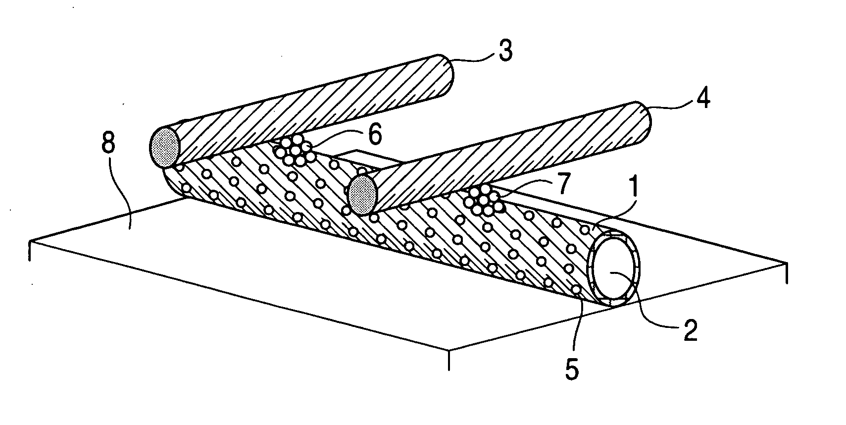
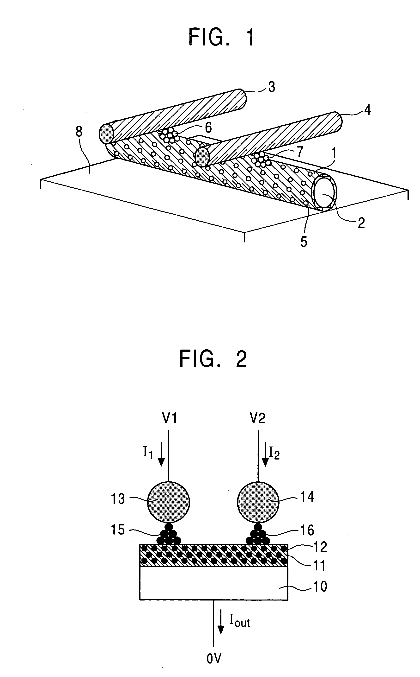
FIG. 2 shows a schematic view of a point contact array according to the present invention, the point contact array being applied to a multiple memory device.

For the sake of simplification, a sample comprising two point contacts is used in a manner similar to FIG. 1. In this case, Ag2S is used as an electronic / ionic mixed conductive material 11 functioning as a first electrode and an Ag wire is used as a metallic wire 10. Pt wires are used as metallic wires 13 and 14 each functioning as a second electrode. The first electrode is grounded and voltages V1 and V2 are independently applied to the second electrodes 13 and 14, respectively. When negative voltages are used as V1 and V2, Ag atoms 12 contained in the electronic / ionic mixed conductive material 11 are precipitated to form bridges 15 and 16. When positive voltages are used as V1 and V2, the Ag atoms 12 in the bridges 15 and 16 return to the electronic / ionic mixed conductive material ...

second embodiment

the present invention will now be described.

First, an example in which an adding circuit is realized with the configuration shown in the first embodiment will be described.

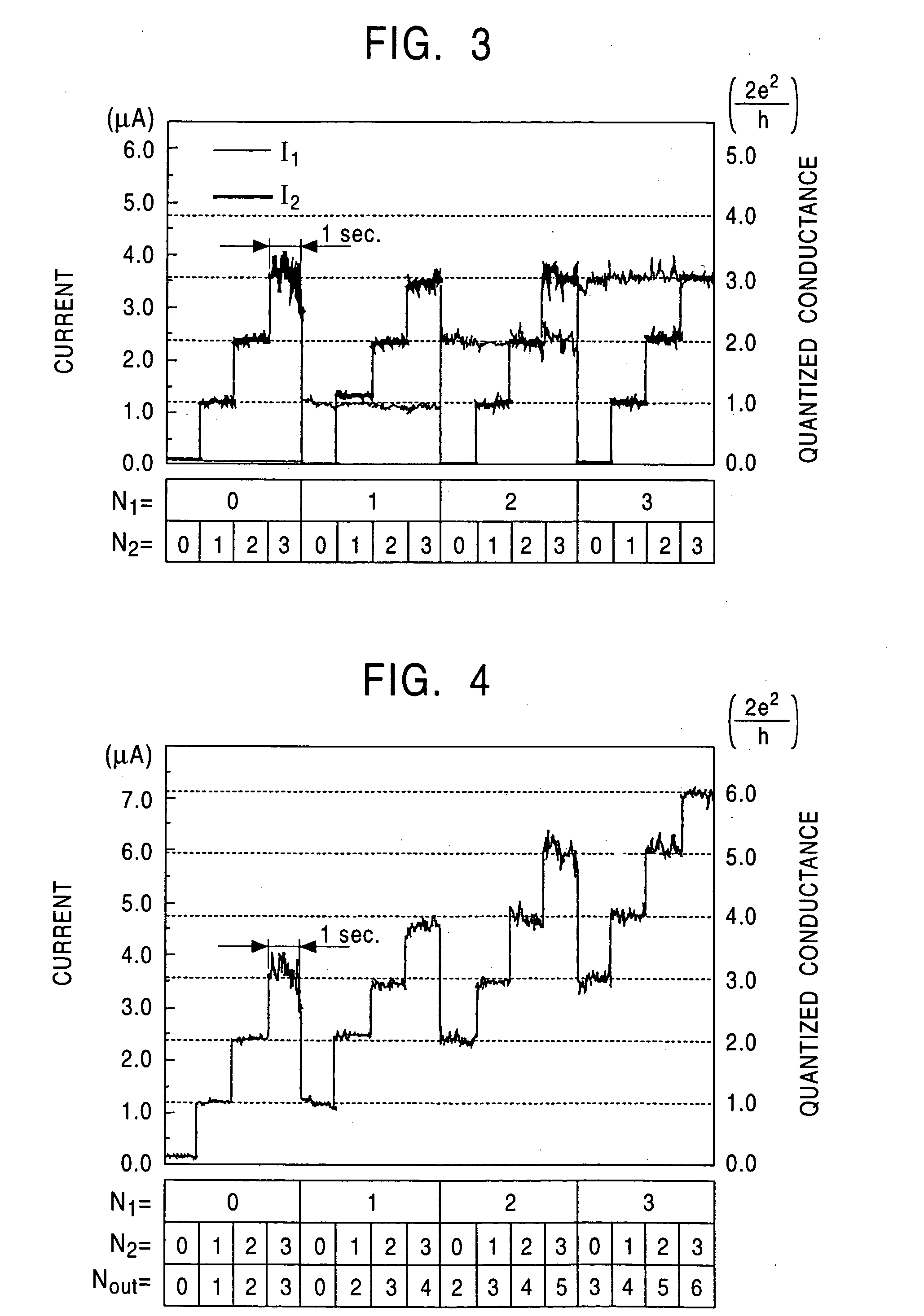
According to the present invention, inputs denote the quantum numbers N1 and N2 of the quantized conductance of the point contacts serving as the bridges 15 and 16. The input operation is performed by controlling the voltages V1 and V2 to set each of N1 and N2 to a desired value. V1 and V2 are set to a reading voltage, for example, 10 mV and a current Iout flowing from the first electrode 10 to a ground potential is measured, thus obtaining the result of an arithmetic operation.

FIG. 4 shows the result of the arithmetic operation according to the second embodiment of the present invention. Below a graph, the inputted N1 and N2 and measured Nout are shown so as to correspond to the abscissa axis of the graph. It is found that the obtained current Iout has quantized conductance corresponding to (N1+N2). In other ...

third embodiment

the present invention will now be described.

The configuration shown in the first embodiment can also be applied to a subtracting circuit. Inputs are controlled by the same method described in the second embodiment. Upon subtraction, voltages, which have the same absolute value and whose polarities are opposite to each other, can be used as V1 and V2. For example, when V1 is set to 10 mV and V2 is set to −10 mV, the current Iout corresponding to quantized conductance, which corresponds to (N1−N2), flows from the first electrode to the ground potential. At that time, when the current flows in the direction from the first electrode to the ground potential, the result of the arithmetic operation indicates a positive value. When the current flows in the direction from the ground potential to the first electrode, the result of the arithmetic operation indicates a negative value.

FIG. 5 shows the result of the arithmetic operation according to the third embodiment.

The arithmetic operati...


PUM


Abstract

A NOT circuit realized using an atomic switch serving as a two terminal device and including a first electrode made of a compound conductive material having ionic conductivity and electronic conductivity and a second electrode made of a conductive substance. Ag2S, Ag2Se, Cu2S, or Cu2Se is preferably used as the compound conductive material.

Description

TECHNICAL FIELD The present invention relates to a point contact array comprising a plurality of devices in each of which a point contact is formed or disconnected between electrodes facing each other to control conductance, a NOT circuit, and an electronic circuit using the same, and more particularly to a NOT circuit comprising an electronic device (an atomic switch which will be described below) in which a point contact is formed or disconnected between electrodes facing each other to control conductance, and an electronic circuit using the same. BACKGROUND ART As related arts [1], methods for forming a point contact to control conductance are disclosed by, for example, J. K. Gimzewski and R. Moller: Phys. Rev. B36, p1284, 1987, J. L. Costa-Kramer, N. Garcia, P. Garcia-Mochales, P. A. Serena, M. I. Marques, and A. Corrcia: Phys. Rev. B55, p5416, 1997, and H. Ohnishi, Y. Kondo, and K. Takayanagi: Nature, Vol. 395, p780, 1998. Each of these methods requires a piezo device in ord...

Claims


Application Information

Patent Timeline
Patent Type & Authority Applications(United States)
IPC IPC(8): G11C11/56G11C13/02G11C16/02H01L27/24H01L27/28H01L29/24H01L29/26H01L29/45H01L51/00H01L51/30H03K19/02
CPCB82Y10/00H03K19/02G11C13/0004G11C13/0009G11C13/0011G11C13/025G11C2213/77G11C2213/81H01L27/2463H01L29/242H01L29/26H01L29/45H01L45/085H01L45/1266H01L45/142H01L45/143H01L45/146H01L45/1633H03K17/545G11C11/5614H10B63/80H10N70/245H10N70/8416H10N70/8822H10N70/8825H10N70/028H10N70/8833H01L29/06
Inventor AONO, MASAKAZUHASEGAWA, TSUYOSHITERABE, KAZUYANAKAYAMA, TOMONOBU
Owner JAPAN SCI & TECH CORP
Why Eureka
Try Eureka