Digitally controlled transconductance cell

a transconductance cell, digital control technology, applied in the direction of dc-amplifiers with dc-coupled stages, dc-amplifiers with semiconductor devices/discharge tubes, differential amplifiers, etc., can solve the problems of large overhead in power dissipation, change of linearity, and increase of power dissipation

Active Publication Date: 2005-05-26
SCINTERA NETWORKS
View PDF5 Cites 18 Cited by
  • Summary
  • Abstract
  • Description
  • Claims
  • Application Information

AI Technical Summary

Benefits of technology

[0009] According to one aspect of the present invention, both the aspect ratio of transistors and the current source are varied together to change the transconductance or gain of a transconductance cell. A constant ratio is maintained, where the ratio is the ratio of the current and the transistor size or aspect ratio [I/(W/L)]. This ratio determines the gate-to-source overdrive voltage of the device, i.e., ΔV=(Vgs−Vth), which determines the linearity of the device. Accordingly, the ratio can be determined based on the linearity requirement so that th...

Problems solved by technology

This, however, changes the linearity and increases power dissipation.
The large increase in the drain current results in a large overhead in power dissipation.
The voltage headroom (Vds, viz. drain to source voltage of a MOS transistor) is also lowered and the variation in linearity is dis...

Method used


Image

  • Digitally controlled transconductance cell
  • Digitally controlled transconductance cell
  • Digitally controlled transconductance cell

Examples


Embodiment Construction

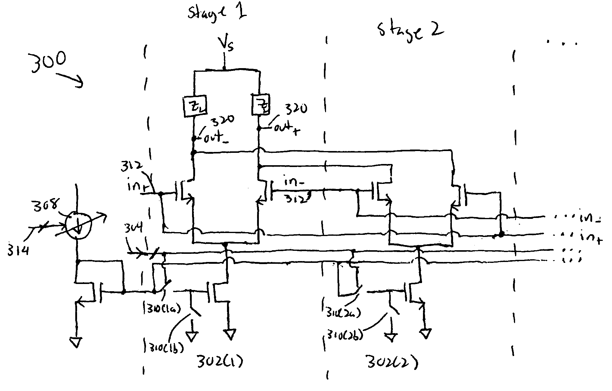
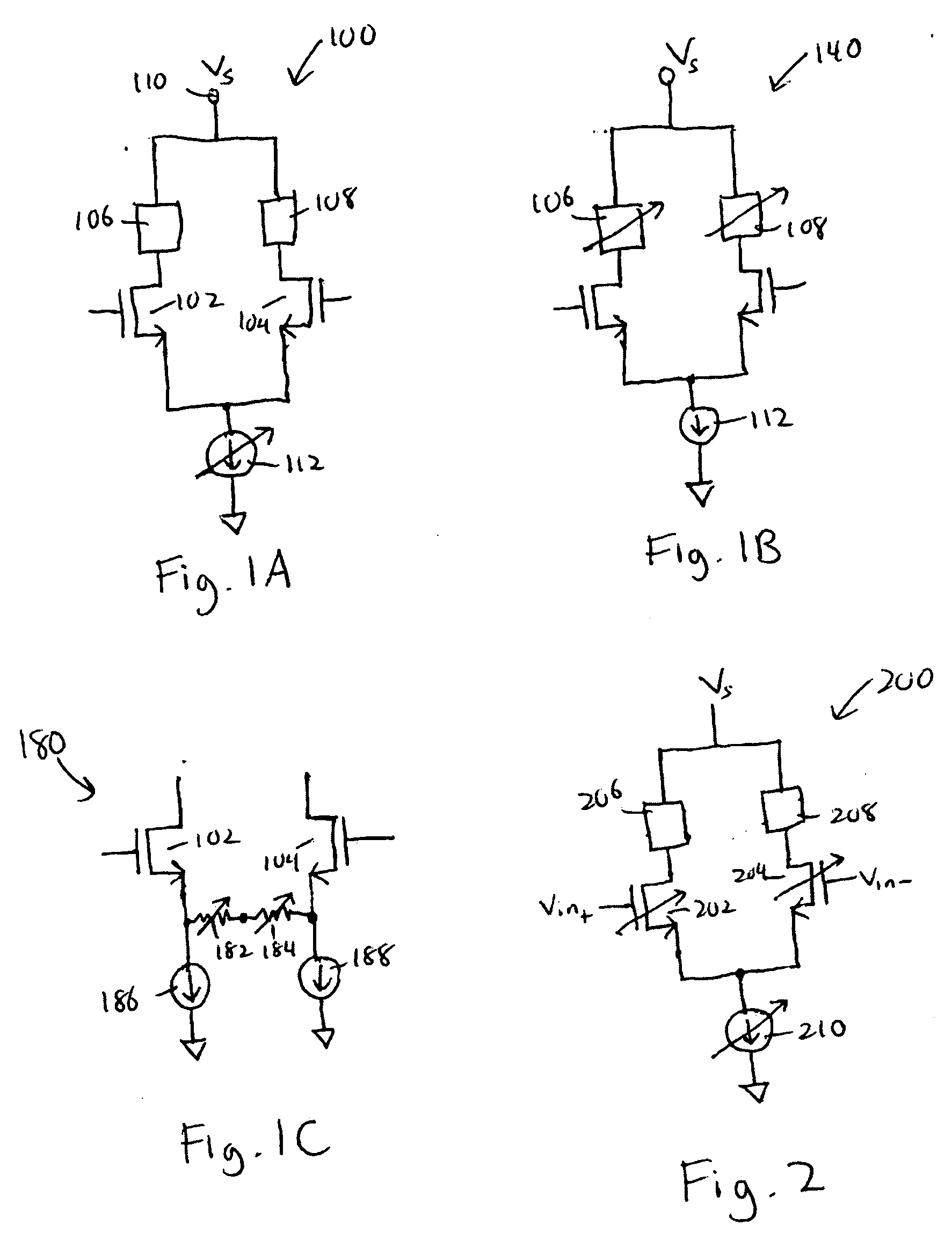
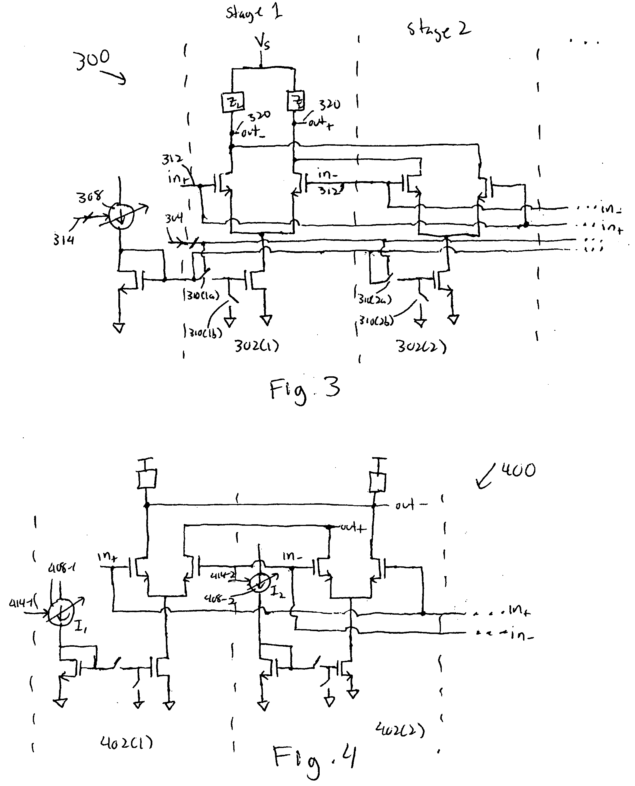
[0020] According to one aspect of the invention, a transconductance cell includes two variable sized transistors, a variable bias current source coupled to the sources of the two transistors, and two resistive load elements coupled to respective drains of the two transistors. The transconductance gm of the cell is varied by changing the size (or aspect ratio) of the transistors and the bias current. In one embodiment, the load elements may also be variable.

[0021]FIG. 2 shows a transconductance cell 200 according to one embodiment of the present invention. Transconductance cell 200 is formed with two transistors 202 and 204, such as N-channel MOS transistors (as shown) or P-channel MOS transistors. The drain of transistors 202 and 204 are each coupled to one terminal of a load element 206 and 208, with the other terminal coupled to a voltage source Vs. Load elements 206 and 208 may be any suitable load having a resistance RL or impedance ZL, as will be discussed below. The load may ...


PUM


Abstract

A digitally controlled transconductance cell includes a differential transistor pair coupled to load elements (either passive or active with resistive or impedance loads) and a variable bias current source, where the transconductance or gain is digitally varied by changing the aspect ratio of the transistors and the bias current.

Description

BACKGROUND [0001] 1. Field of the Invention [0002] The present invention relates to electrical circuits, and in particular, to transconductance cells. [0003] 2. Related Art [0004] As is known in the art, a transconductance cell is a basic electrical circuit or block used to build more complex electrical circuits, such as low noise amplifiers and analog filters. The transconductance cell performs the function of converting a voltage input into different current outputs, such as by varying the transconductance gm of the cell (iout=gm*Vin). The characteristics of a desirable transconductance cell include high bandwidth, low power consumption, high output impedance, low distortion, and good common mode rejection. Furthermore, with an ever-increasing need and use of high speed analog circuits and chips, transconductance cells should be able to provide these characteristics at high speeds with wide linear dynamic range and low power dissipation. [0005]FIG. 1A shows a conventional transcon...

Claims


Application Information

Patent Timeline
IPC IPC(8): H03F3/45
CPCH03F3/45183H03F2200/372H03F2203/45362H03F2203/45466H03F2203/45731H03F2203/45508H03F2203/45631H03F2203/45638H03F2203/45662H03F2203/45504
Inventor BHATTACHARJEE, JISHNUMUKHERJEE, DEBANJANPHANSE, ABHIJIT
Owner SCINTERA NETWORKS
Why Eureka
Try Eureka