
Method for manufacturing semiconductor devices and plug
a manufacturing method and technology for semiconductor devices, applied in the direction of semiconductor devices, basic electric elements, electrical equipment, etc., can solve the problems of increasing the difficulty of manufacturing process, increasing the demand for size precision, and exposure of other component devices, so as to prevent current leakage or abnormal electrical performance. , the effect of increasing the number o
- Summary
- Abstract
- Description
- Claims
- Application Information
AI Technical Summary
Benefits of technology
Problems solved by technology
Method used
Image

Examples
first embodiment
The First Embodiment
[0020] According to the present invention, the foregoing general description and the following detailed description of an embodiment with reference to the accompanying drawings are exemplary and explanatory for a plug fabrication of a trench type flash memory process. This invention, however, may be embodied in many different forms and should not be construed as limited to the embodiments set forth herein. The present invention is applicable to any process that is related to the formation of a plug in a dielectric layer, wherein the plug is electrically connected to an adjacent device underneath.
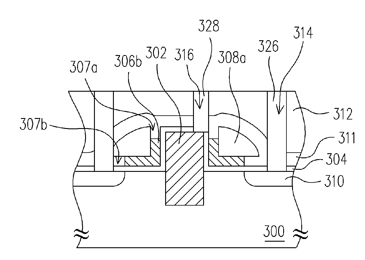
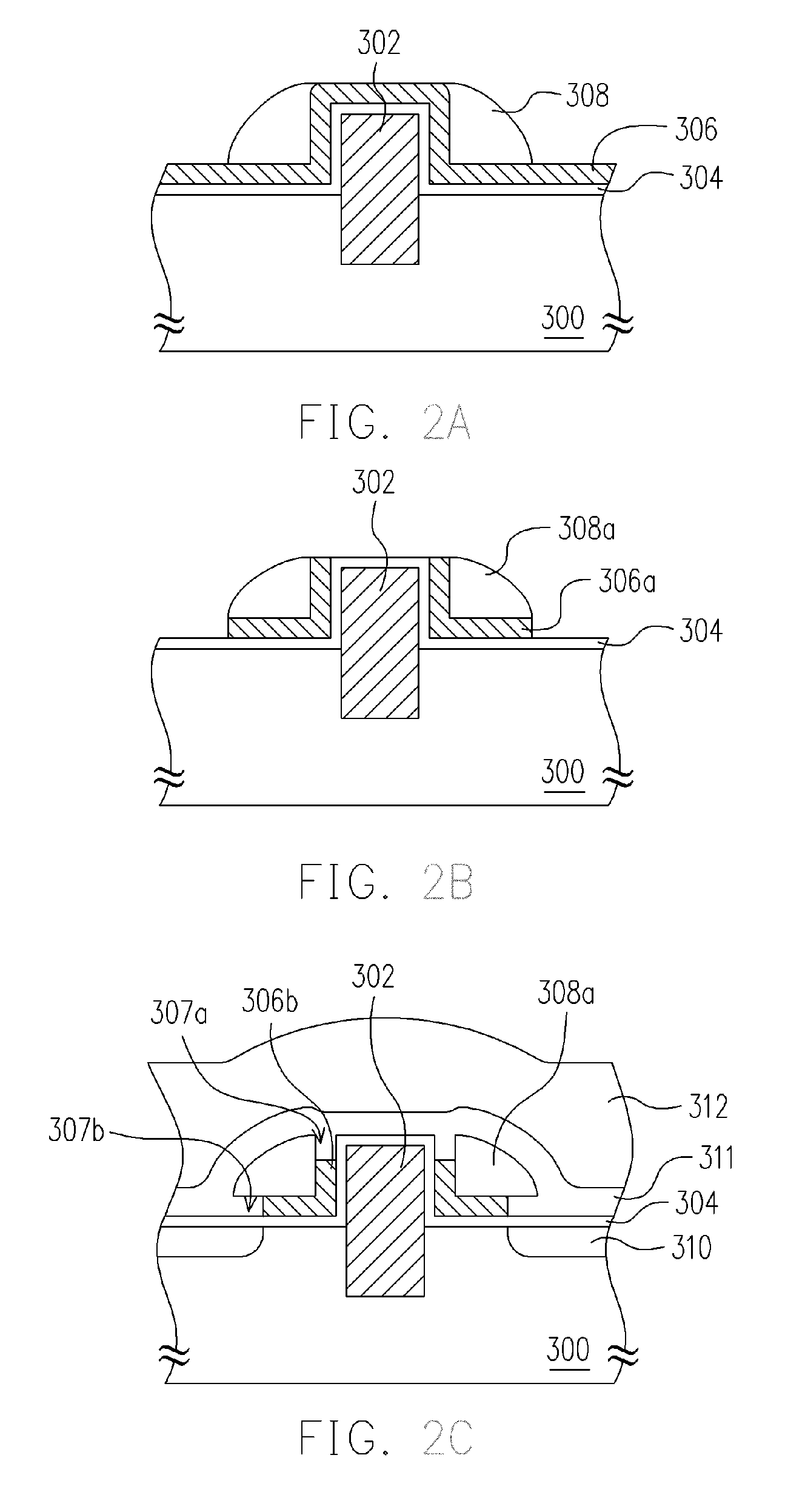
[0021]FIG. 2A to FIG. 2D are schematic cross sectional views showing the steps for fabricating a plug according to an embodiment of the present invention, wherein the plug is formed in the dielectric layer and is electrically connected to the trench type flash memory.
[0022] Please referring to FIG. 2A, a substrate 300 that includes the trench gate structure 302 is provi...
second embodiment
The Second Embodiment
[0030] According to the present invention, the foregoing general description and the following detailed description of the embodiment with reference to the accompanying drawings are exemplary and explanatory for the fabrication of plugs during the interconnect processing. This invention, however, may be embodied in many different forms and should not be construed as limited to the embodiments set forth herein. The present invention is applicable to any process that is related to the formation of a plug in a dielectric layer, wherein the plug is electrically connected to an adjacent device underneath.
[0031]FIG. 3A to FIG. 3D are schematic cross sectional views showing the steps of fabrication of a plug fabrication in an interconnect manufacturing process according to another embodiment of the present invention, wherein the plug is formed in the dielectric layer and is electrically connected to the conducting structure at the lower level.
[0032] Please referring ...
PUM
 Abstract
Description
Claims
Application Information