

Light-emitting device, liquid-crystal display device and method for manufacturing same
a technology of liquid crystal display and light-emitting device, which is applied in the direction of organic semiconductor devices, instruments, optics, etc., can solve the problems of increasing interconnection resistance, increasing power consumption, and forming of encounter projections such as whiskers, and achieves low power consumption and reduced line resistance
Patent Information
- Authority / Receiving Office
- US · United States
- Patent Type
- Applications(United States)
- Current Assignee / Owner
- Publication Date
- 2006-08-24
- Estimated Expiration
- Not applicable · inactive patent
Smart Images
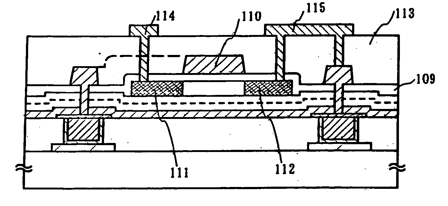
Figure 1 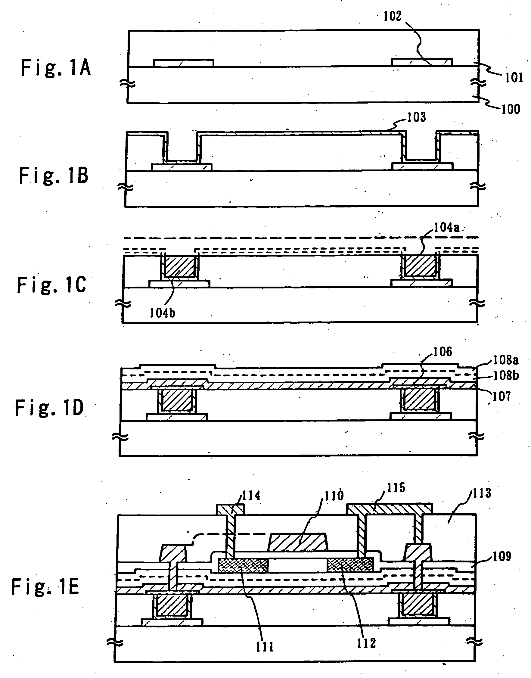
Figure 2 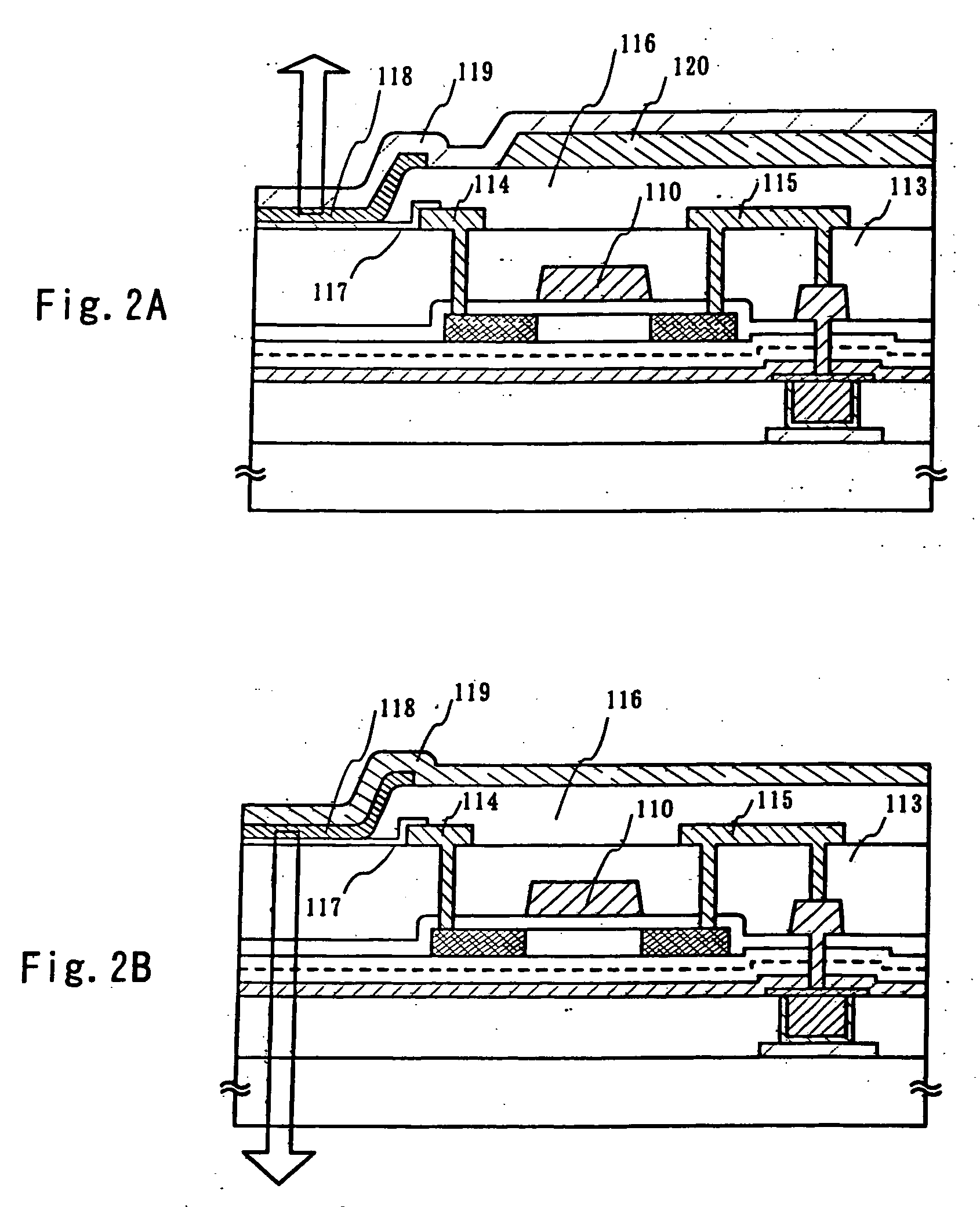
Figure 3
Abstract
Description
BACKGROUND OF THE INVENTION
[0001] 1. Technical Field of the Invention
[0002] The present invention relates to a semiconductor device having a circuit configured with thin-film transistors (hereinafter, referred to as TFTs) and a method for manufacturing same. For example, the invention relates to an electronic apparatus mounting, as a part, an electro-optical device represented by a liquid-crystal display or a light-emitting device having OLEDs.
[0003] Incidentally, the semiconductor device in this description refers to a device as a whole which is capable of functioning by the utilization of a semiconductor characteristic, i.e. electro-optical devices, semiconductor circuits and electronic apparatuses are all fallen under semiconductor devices.
[0004] 2. Description of the Related Art
[0005] Recently, attentions are drawn to the art to structure a thin-film transistor (TFT) by the use of a semiconductor film (thickness: approximately several to several hundred nm) formed over a su...
Examples
example
Example 1
[0093] This example shows that the major part of the power supply line of a light-emitting device is made as a buried interconnection, in FIGS. 3 to 6.
[0094] At first, according to the above embodiment, an etching-stop layer is formed on a substrate having an insulating surface and a silicon-based insulating film is formed covering the etching-stop layer. The insulating film is selectively etched to form an opening (trench) reaching the etching-stop layer. After forming a first barrier layer, electrolytic plating is carried out to form a low-resistance metal film having a sufficient thickness in the opening (trench). Subsequently, planarization represented by the chemical mechanical polishing (hereinafter, referred to as CMP) is made to leave the copper and first barrier layer only in the opening (trench) but remove away unwanted portions, thereby forming an interconnection in a buried form. The top view in this process stage is shown in FIG. 3, wherein the sectional view...
example 2
[0131] This shows an example that the major part of a gate line of a liquid-crystal display device is made by a buried interconnection, in FIGS. 12 and 13.
[0132] At first, according to the above embodiment, an etching-stop layer is formed on a substrate having an insulating surface and a silicon-based insulating film is formed covering the etching-stop layer. The insulating film is selectively etched to form an opening (trench) reaching the etching-stop layer. After forming a first barrier layer, electrolytic plating is carried out to form a low-resistance metal film having a sufficient thickness in the opening (trench). Subsequently, planarization represented by the chemical mechanical polishing (hereinafter, referred to as CMP) is made to leave the copper and first barrier layer only in the opening (trench) but remove away unwanted portions, thereby forming an interconnection in a buried form.
[0133] Then, a second barrier layer is formed in order to provide an exposed portion of...
example 3
[0141] The drive circuit and pixel region formed by carrying out the invention can complete various modules (active-matrix liquid-crystal module, active-matrix EC module). Namely, the invention can complete an electronic apparatus built it in a display part.
[0142] Such electronic apparatuses include video cameras, digital cameras, head-mount displays (goggle type displays), car navigators, projectors, car stereo sets, personal computers, and personal digital assistants (mobile computers, cellular phones or electronic books). Examples of them are shown in FIGS. 14A to 14C and 15A and 15B.
[0143]FIG. 14A is a personal computer, including a main body 2001, an image input part 2002, a display part 2003, a keyboard 2004 and so on.
[0144]FIG. 14B is a mobile computer, including a main body 2201, a camera part 2202, an image receiving part 2203, an operation switch 2204, and a display part 2205.
[0145]FIG. 14C is a player using a recording medium recording a program (hereinafter, referred...