High efficiency inductor, method for manufacturing the inductor, and packaging structure using the inductor

a high-efficiency inductors and manufacturing method technology, applied in the field of inductors, can solve the problems of difficulty in incorporating a device packaging, low quality factor of conventional inductors, and difficulty in manufacturing other devices together, and achieve excellent properties

Active Publication Date: 2007-04-19
SAMSUNG ELECTRONICS CO LTD
View PDF6 Cites 74 Cited by
  • Summary
  • Abstract
  • Description
  • Claims
  • Application Information

AI Technical Summary

Benefits of technology

[0010] The present invention provides an inductor capable of e

Problems solved by technology

However, in view of conventional inductors requiring a considerable amount of space for installation and difficulty in manufacturing conventional inductors due to their complex coil structure, conventional inductors have a low quality factor.
Particularly, in the case that many devices have to be embodied on one wafer, a process of manufacturing other devices together may be difficult due to an inductor an

Method used


Image

  • High efficiency inductor, method for manufacturing the inductor, and packaging structure using the inductor
  • High efficiency inductor, method for manufacturing the inductor, and packaging structure using the inductor
  • High efficiency inductor, method for manufacturing the inductor, and packaging structure using the inductor

Examples


Embodiment Construction

[0031] Reference will now be made in detail to the exemplary embodiments of the present invention, examples of which are illustrated in the accompanying drawings, wherein like reference numerals refer to the like elements throughout. The exemplary embodiments are described below to explain the present invention by referring to the figures.

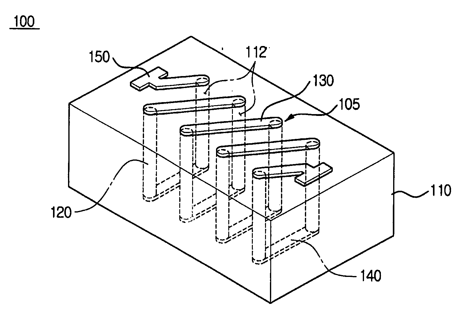
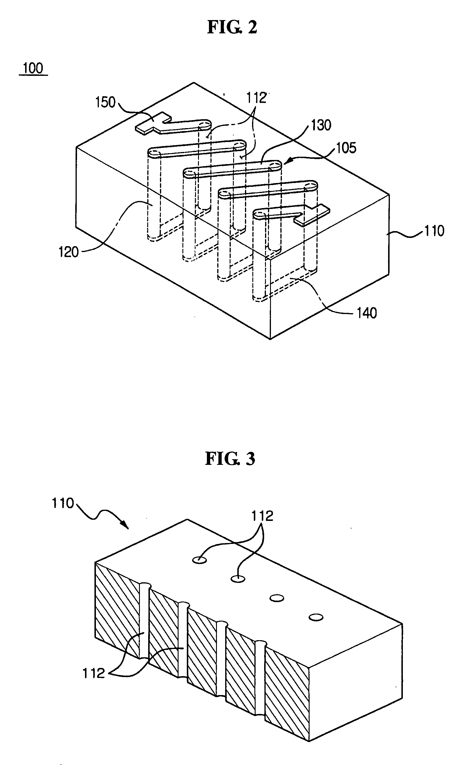
[0032]FIG. 2 is a perspective view illustrating an inductor 100 according to an exemplary embodiment of the present invention.

[0033] Referring to FIG. 2, the inductor 100 includes a substrate 110, vertical conductive portions 120, first horizontal conductive portions 130, second horizontal conductive portions 140, and electrode portions 150. The vertical conductive portions 120 pass through the body of the substrate 110 and are exposed at the top and the bottom of the body of the substrate 110. The first and second horizontal conductive portions 130 and 140, respectively, electrically connect the exposed vertical conductive portions 120 to provid...


PUM


Abstract

An inductor is provided which includes a plurality of via holes vertically passing through a substrate, the substrate having insulating properties, vertical conductive portions filling the via holes, and horizontal conductive portions connecting each individual vertical conductive portions at the top and the bottom of the substrate to form a single coil structure with the vertical conductive portions.

Description

CROSS-REFERENCE TO RELATED APPLICATIONS [0001] This application claims priority from Korean Patent Application No. 10-2005-98595, filed on Oct. 19, 2005, in the Korean Intellectual Property Office, the disclosure of which is incorporated herein in its entirety by reference. BACKGROUND OF THE INVENTION [0002] 1. Field of the Invention [0003] The present invention relates to an inductor, and more particularly, to a spiral inductor having a micro size and high efficiency, a method of manufacturing the inductor, and a device package structure using the inductor as a packaging element. [0004] 2. Description of the Related Art [0005] An inductor is one of the most important components forming an electric circuit, along with a resistor, a condenser, an electron tube, a transistor, and a power source, and has a coil structure in which copper or aluminum is wound in the shape of a screw several times. The inductor can suppress a sudden change of a current by inducing voltage in proportion to...

Claims


Application Information

Patent Timeline
IPC IPC(8): H01F5/00
CPCH01F17/0033H01F41/041H01F2017/002H01L27/08H01L28/10H01F27/30
Inventor LEE, MOON CHULKWON, JONG OHKIM, WOON BAEHWANG, JUN SIKMOON, CHANG YOULSONG, IN SANG
Owner SAMSUNG ELECTRONICS CO LTD
Why Eureka
Try Eureka