Display substrate, display apparatus having the display substrate and method for manufacturing the display apparatus

a technology of display apparatus and substrate, which is applied in the direction of semiconductor devices, semiconductor/solid-state device details, instruments, etc., can solve the problems of increasing the manufacturing cost of the lcd apparatus, and achieve the effect of reducing the thickness and weight of the display apparatus and reducing the manufacturing cost of the display apparatus

Inactive Publication Date: 2008-01-24
SAMSUNG ELECTRONICS CO LTD
View PDF11 Cites 25 Cited by
  • Summary
  • Abstract
  • Description
  • Claims
  • Application Information

AI Technical Summary

Benefits of technology

[0008]Embodiments of the present invention provide a display substrate capable of reducing manufacturing processes and costs thereof, a display apparatus having the display substrate, and a method for manufacturing the display apparatus.
[0013]According to embodiments of the present invention, a polarizing member is formed inside the display apparatus, so that a thickness and a weight of the display apparatus may be decreased and manufacturing costs of the display apparatus may be decreased.

Problems solved by technology

However, since the LCD apparatus displays an image by using a liquid crystal layer as a light shutter, the LCD apparatus requires linearly polarized light to display an image.
Since a price of the polarizing plate attached to the LCD apparatus is high manufacturing costs of the LCD apparatus increases.

Method used


Image

  • Display substrate, display apparatus having the display substrate and method for manufacturing the display apparatus
  • Display substrate, display apparatus having the display substrate and method for manufacturing the display apparatus
  • Display substrate, display apparatus having the display substrate and method for manufacturing the display apparatus

Examples


Embodiment Construction

[0025]The invention is described more fully hereinafter with reference to the accompanying drawings, in which embodiments of the invention are shown. This invention may, however, be embodied in many different forms and should not be construed as limited to the embodiments set forth herein.

[0026]It will be understood that when an element or layer is referred to as being “on,”“connected to” or “coupled to” another element or layer, it can be directly on, connected or coupled to the other element or layer or intervening elements or layers may be present.

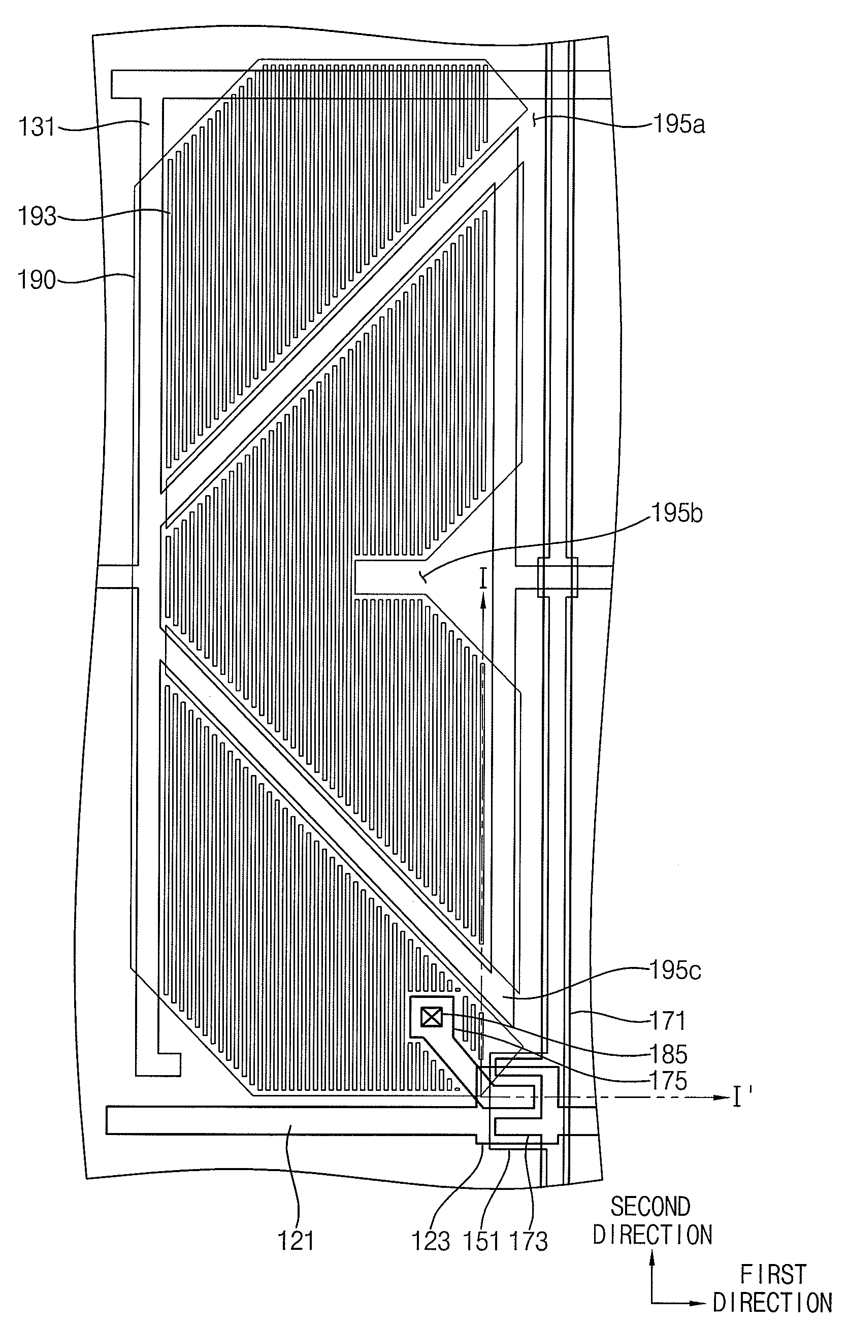
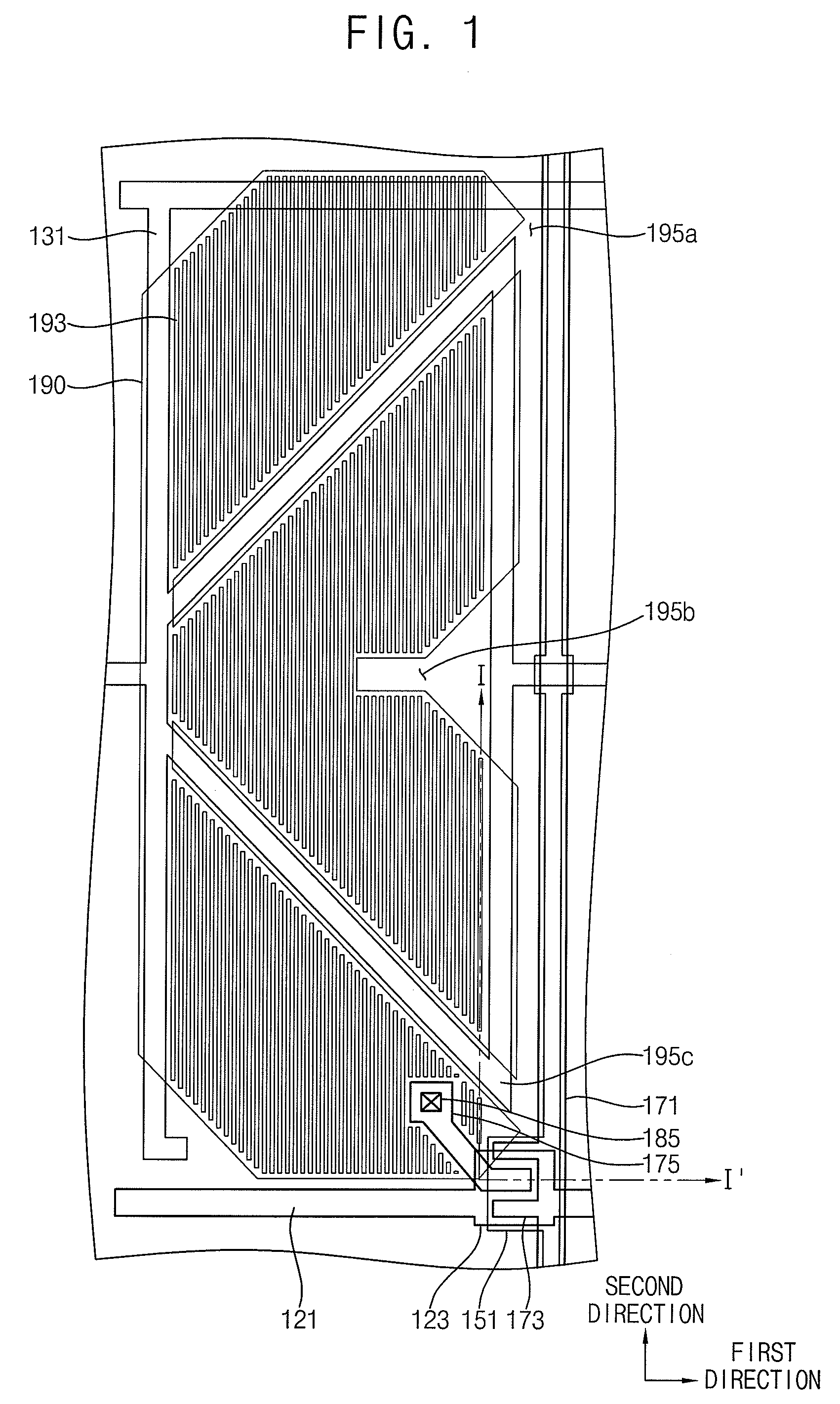
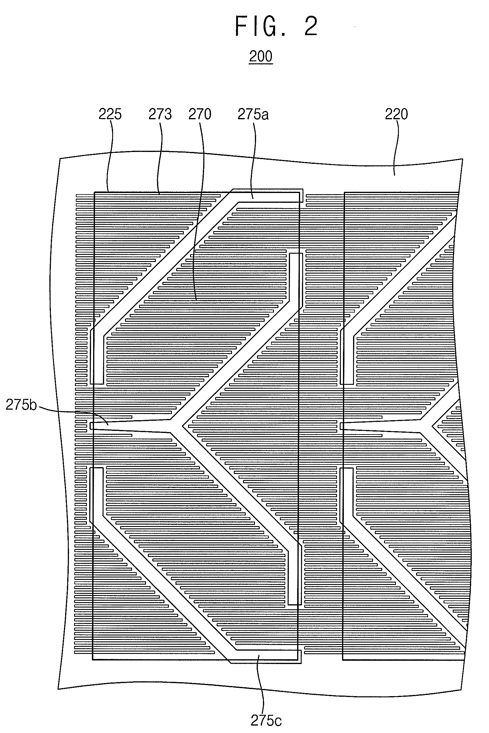
[0027]FIG. 1 is a plan view illustrating a thin film transistor (TFT) display substrate according to an exemplary embodiment of the present invention. FIG. 2 is a plan view illustrating a common electrode display substrate according to an exemplary embodiment of the present invention. FIG. 3 is a cross-sectional view illustrating a display apparatus including the TFT display substrate shown in FIG. 1 and the common electrode display sub...


PUM


Abstract

A display apparatus includes a first substrate, a gate line formed on the first substrate, a gate insulating layer formed on the gate line, a semiconductor layer formed on the gate insulating layer, a data line formed on the semiconductor layer and including a source electrode, a drain electrode facing the source electrode, a first electrode electrically connected to the drain electrode, in a second substrate facing the first substrate, a second electrode formed on the second substrate, and a liquid crystal layer disposed between the first electrode and the second electrode. At least one of the first and second electrodes includes a plurality of line patterns to polarize incident light.

Description

CROSS-REFERENCE TO RELATED APPLICATION[0001]This application claims priority to Korean Patent Application No. 2006-68334, filed on Jul. 21, 2006 the disclosure of which is incorporated herein by reference in its entirety.BACKGROUND OF THE INVENTION[0002]1. Technical Field[0003]The present invention relates to a display substrate, a display apparatus having the display substrate and a method for manufacturing the display apparatus, and more particularly, to a display substrate capable of reducing manufacturing processes and costs thereof.[0004]2. Discussion of the Related Art[0005]A liquid crystal display (LCD) apparatus is more commonly used than a cathode ray tube (CRT) display apparatus, since a thickness of the LCD apparatus is thinner than the CRT display apparatus, and a weight of the LCD apparatus is lighter than the CRT display apparatus. However, since the LCD apparatus displays an image by using a liquid crystal layer as a light shutter, the LCD apparatus requires linearly ...

Claims


Application Information

Patent Timeline
Patent Type & Authority Applications(United States)
IPC IPC(8): H01L27/13H01L21/3205H01L23/48
CPCG02F1/133528H01L27/12G02F2001/133548G02F1/134336G02F1/133548G02F1/1335G02F1/1343
Inventor JEONG, CHANG-OHKIM, SANG-GABSOUK, JUN-HYUNGKIM, HONG-GYUNHWANG, IN-SUNOH, MIN-SEOKCHIN, HONG-KEEJEONG, YU-GWANGCHOI, SEUNG-HALEE, HI-KUKKIM, SHI-YUL
Owner SAMSUNG ELECTRONICS CO LTD
Why Eureka
Try Eureka