Image sensor ADC and CDS per Column with Oversampling

a technology of image sensor and column, applied in the field of solid-state imaging devices, can solve the problems of large-bus analog multiplexing, high undesired power consumption of the entire array, and large noise of analog current, and achieve the effect of reducing the available area

Active Publication Date: 2008-02-21
DYNAMAX IMAGING
View PDF8 Cites 74 Cited by
  • Summary
  • Abstract
  • Description
  • Claims
  • Application Information

AI Technical Summary

Benefits of technology

[0016] Accordingly, it is an object of the present invention to provide a straightforward technique for converting the video pixel signals from a solid state imaging device to a digital video signal, and to achieve the same effect on-chip with an array that consumes a minimum of available area, and which avoids drawbacks of the prior art.

Problems solved by technology

Wide-bus analog multiplexing has significant problems due, for example, to highly capacitive loads, long settling times, voltage drop across the bus, noise cross-coupling from neighboring circuits.
That surge in the analog current can inject a significant amount of noise to the highly sensitive pixel site or pixel amplifier voltage storage nodes.
Finally, if the arrayed analog buffer has to be able to drive the capacitive bus (even at moderate speeds) it will need a higher quiescent supply current in the output stage and that current gets multiplied by the number of arrayed elements to yield a very high undesired power consumption for the entire array.
A serious problem for analog arrayed circuits is that any mismatch between the devices will appear as fixed pattern noise (i.e., offset variations from one circuit in the array to the next).
As the analog array pitch decreases it becomes difficult or impossible to achieve proper device matching by the usual technique making large devices, placing them in proximity and utilizing dummy devices in order to make dependant devices similar in their electric parameters.
This problem, however, would be absent in digital implementations.
Thus the SAR ADC suffers deficiencies with respect to size, accuracy and power consumption.
However, this is still an SAR design, and consumes much of the available device area.
With the prior techniques, it is difficult to reduce the size of the analog portions of the digitizing circuitry.
That technique requires temporary storage of intermediate information, so as to permit the combining of the pixel information with the different integration times, thus creating additional system complexity.
The technique of that patent also has the problem that the readouts for the same pixel will have non-overlapping integration times, leading to image blur when the different integration periods are combined.

Method used


Image

  • Image sensor ADC and CDS per Column with Oversampling
  • Image sensor ADC and CDS per Column with Oversampling
  • Image sensor ADC and CDS per Column with Oversampling

Examples


Embodiment Construction

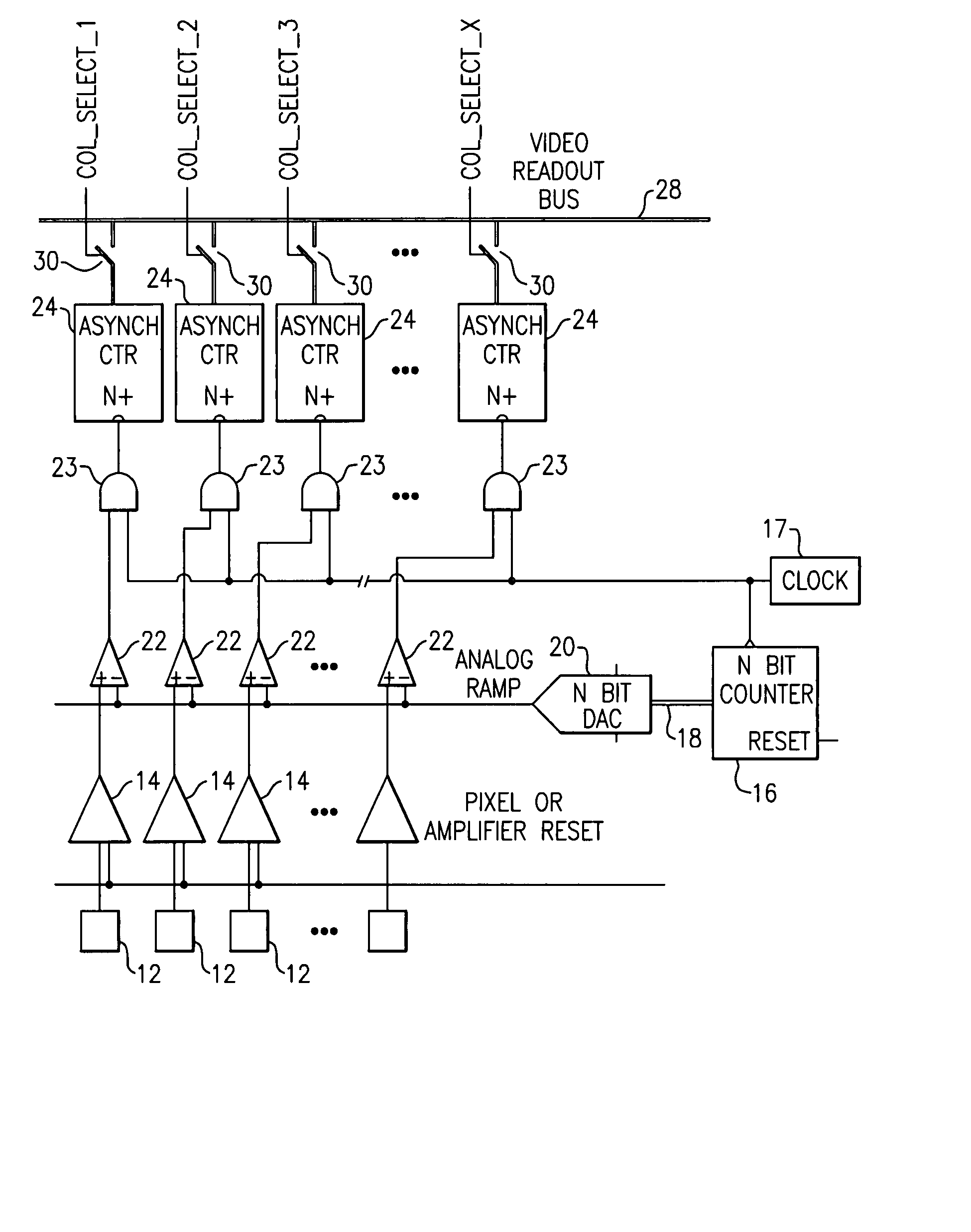
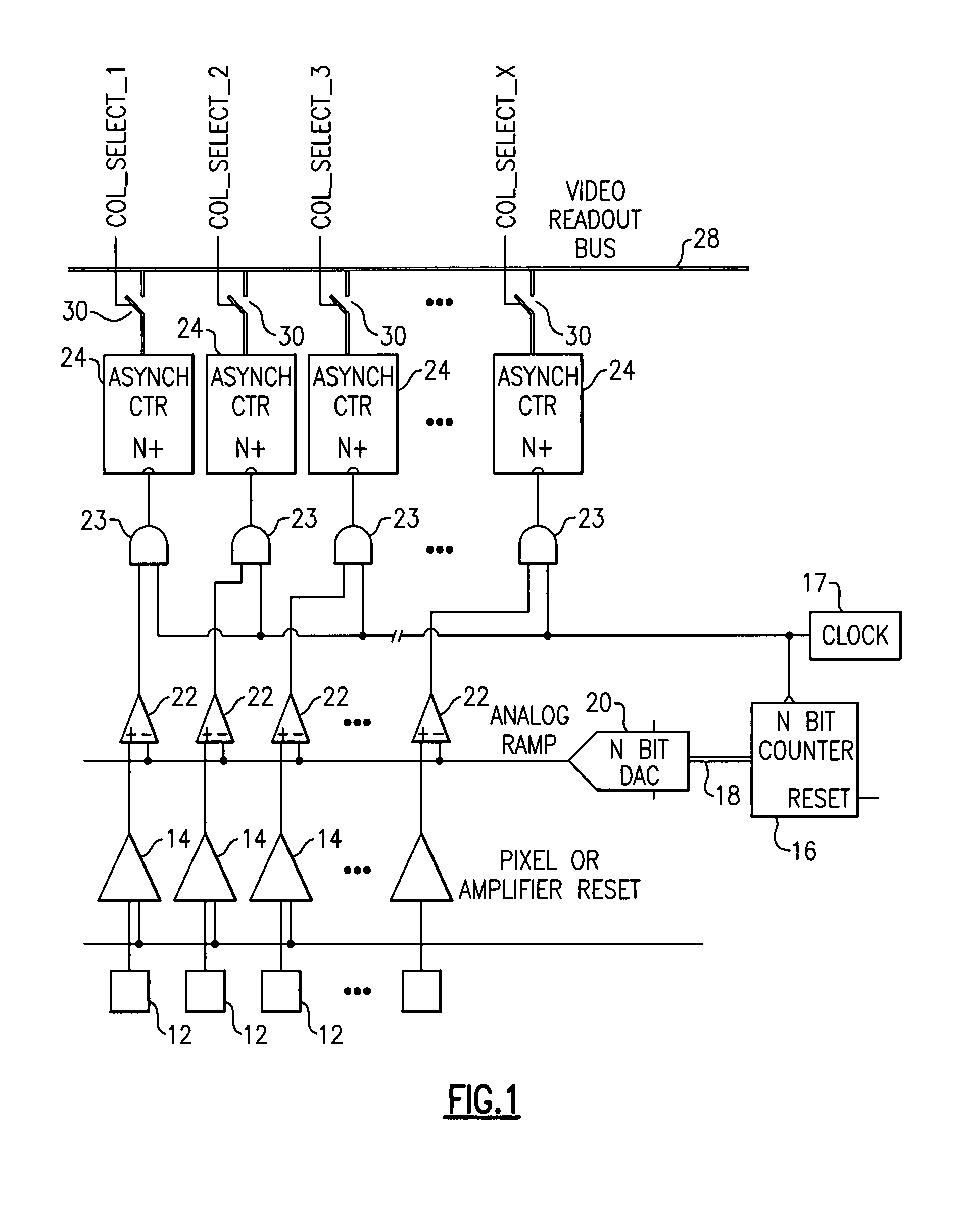
[0057] With reference to the Drawing figures, and initially to FIG. 1 thereof, an arrayed solid-state imager 10 is shown, which incorporates an N-bit ADC conversion facility that employs an N-bit counter and a DAC to generate an analog ramp.

[0058] In this imager 10, there are multiple columns, each comprising one or more pixels 12. In this case the pixel 12 represents one or multiple pixels of the same column, and each pixel 12 is connected with an input of a column amplifier 14. A pixel reset line is also connected to a reset input of each of the column amplifiers 14. An N-bit counter 16 counts up clock signals that are supplied from a clock pulse generator 17, and the counter 16 supplies a digital count value on a counter output bus 18 that supplies an input of a DAC or digital-to-analog converter element 20. For simplicity, the same clock pulse generator 17 is used for both the counter / latches 24 and the DAC 20. The user may employ different clock pulse generators to add flexibi...


PUM


Abstract

A solid state imager converts analog pixel values to digital form on an arrayed per-column basis. An N-bit counter supplies an N-bit DAC to produce an analog ramp output with a level that varies corresponding to the contents of the counter. A latch/counter or equivalent is associated with each respective column. A clock supplies clock signal(s) to the counter elements. When the analog ramp equals the pixel value for that column, the latch/counter latches the value. The black level can be pre-set in the latch/counter or can be subtracted separately to reduce fixed pattern noise. The pixels can be oversampled for some number of times, e.g., n=16, to reduce the thermal noise of the sensors. Also, two or more pixels sharing a common sense node may be binned together, and two (or more) pixels having different integration times may be combined to obtain an output signal with enhanced dynamic range.

Description

[0001] This is a Continuation-in-Part of earlier co-pending and commonly assigned U.S. patent application Ser. No. 11 / 230,385, filed Sep. 20, 2005, which is a Continuation-in-Part of application Ser. No. 10 / 106,399, filed Mar. 25, 2002, now U.S. Pat. No. 6,965,407, which claims priority of Provisional Application Ser. No. 60 / 278,639, Mar. 26, 2001, now abandoned.BACKGROUND OF THE INVENTION [0002] This invention relates to solid state imaging devices, and is more specifically directed to an imager that converts analog pixel values to corresponding digital values on an arrayed basis, with significantly reduced circuitry. The invention is also concerned with compensation of errors that may be present in conversion, as well as correction for offset errors attributable to the pixel photo sensor areas or to the pixel amplifiers. [0003] The invention is also concerned with a distributed analog-to-digital converter arrangement, i.e., distributed one per pixel, which allows for oversampling ...

Claims


Application Information

Patent Timeline
Patent Type & Authority Applications(United States)
IPC IPC(8): H04N5/335H03M1/12H03M1/56H04N5/347H04N5/355H04N5/365H04N5/3745
CPCH03M1/1019H03M1/123H03M1/1235H03M1/56H04N5/378H04N5/335H04N5/3742H04N5/37455H04N5/3765H04N3/1575H04N25/00H04N25/616H04N25/767H04N25/772H04N25/745H04N25/75
Inventor POONNEN, THOMASZARNOWSKI, JEFFREY J.LIU, LIJOYNER, MICHAELKARIA, KETAN V.
Owner DYNAMAX IMAGING
Why Eureka
Try Eureka