
Detecting circuit, modulation scheme identifying circuit, integrated circuit, tuning device, and common multi-scheme receiving device
a modulation scheme and detecting circuit technology, applied in the direction of amplitude demodulation, line-fault/interference reduction, baseband system details, etc., can solve the problems of generating unnecessary interference signals, demodulating circuits which are not receiving signals, and wasting power, so as to reduce the power consumption of the detecting circuit and reduce the circuit size and power consumption.
- Summary
- Abstract
- Description
- Claims
- Application Information
AI Technical Summary
Benefits of technology
Problems solved by technology
Method used
Image

Examples
Embodiment Construction
[0037]The following will describe embodiments of the present invention in reference to the figures. Here, for convenience, the members that have the same arrangement and function as those shown in FIG. 5 are indicated by the same reference numerals and their description may be entirely or partly omitted.
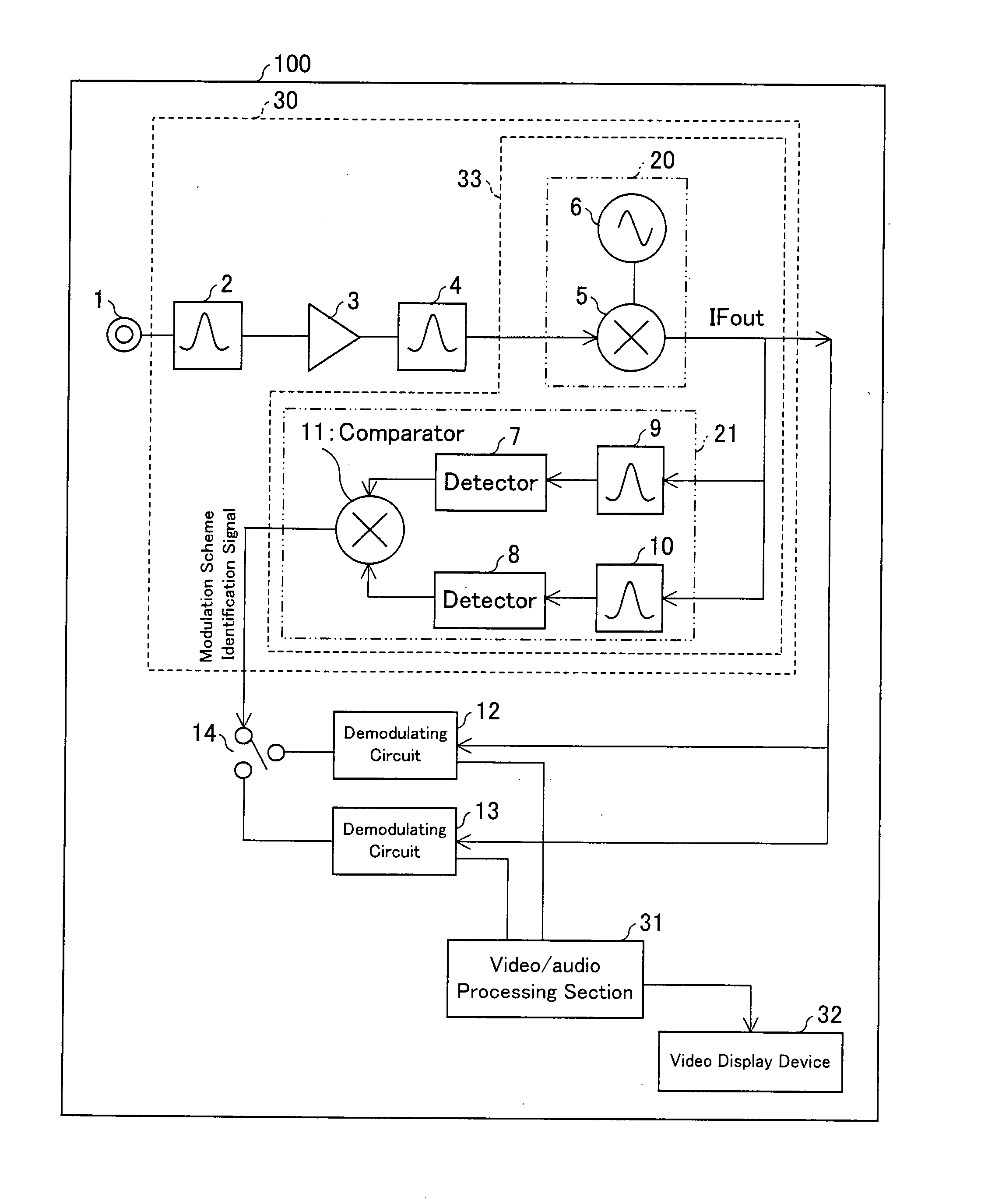
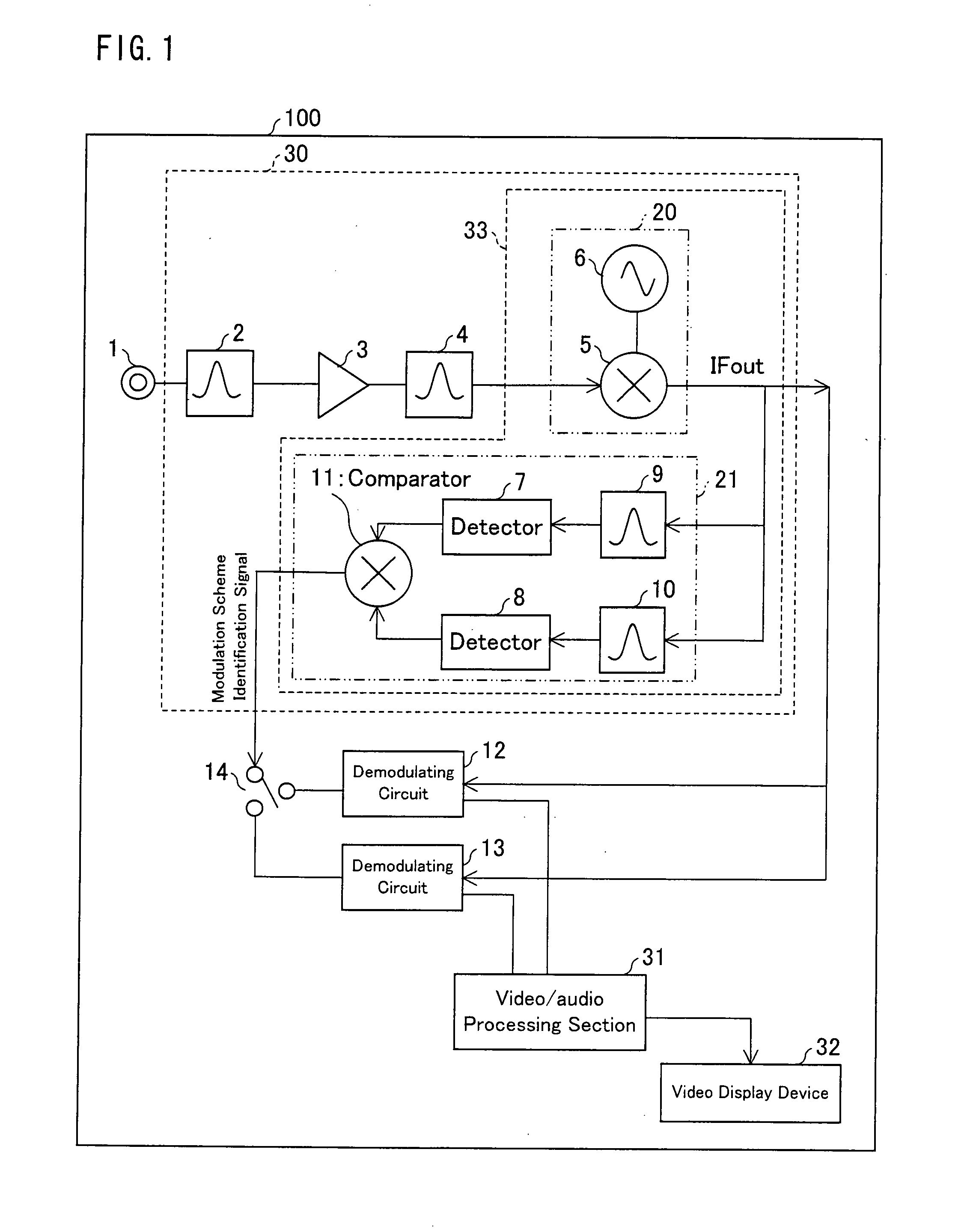
[0038]FIG. 1 is a block diagram illustrating the structure of a detecting circuit in a common multi-scheme receiving device 100 in accordance with the present embodiment. The common multi-scheme receiving device 100 shown is a television broadcast receiving device which receives terrestrial digital broadcast and terrestrial analog broadcast to produce video and audio outputs.
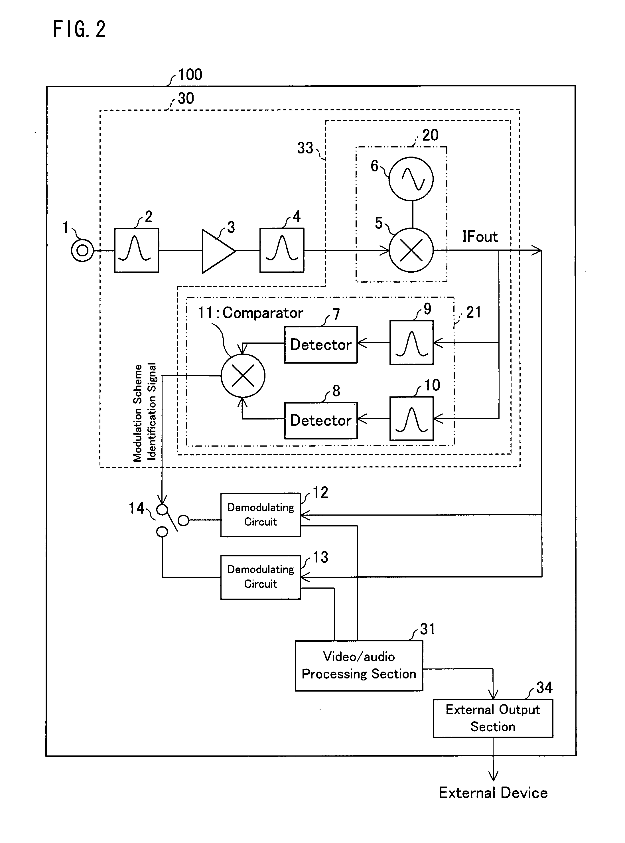
[0039]As shown in the figure, the common multi-scheme receiving device 100 contains a receiver antenna 1, a tuning device 30, demodulating circuits 12, 13, a control circuit 14, a video / audio processing circuit 31, and a video display device 32. The tuning device 30 contains an input tuning circuit 2, a high freq...
PUM
 Abstract
Description
Claims
Application Information