

Single wafer processing unit
a processing unit and single wafer technology, applied in the direction of liquid surface applicators, pretreated surfaces, coatings, etc., can solve problems such as transmission errors, and achieve the effects of preventing the generation of cambering deformation, and reducing the risk of transmission errors
- Summary
- Abstract
- Description
- Claims
- Application Information
AI Technical Summary
Benefits of technology
Problems solved by technology
Method used
Image

Examples
Embodiment Construction
[0046]Hereinafter, an embodiment of a processing unit according to the present invention is described in detail with reference to attached drawings.
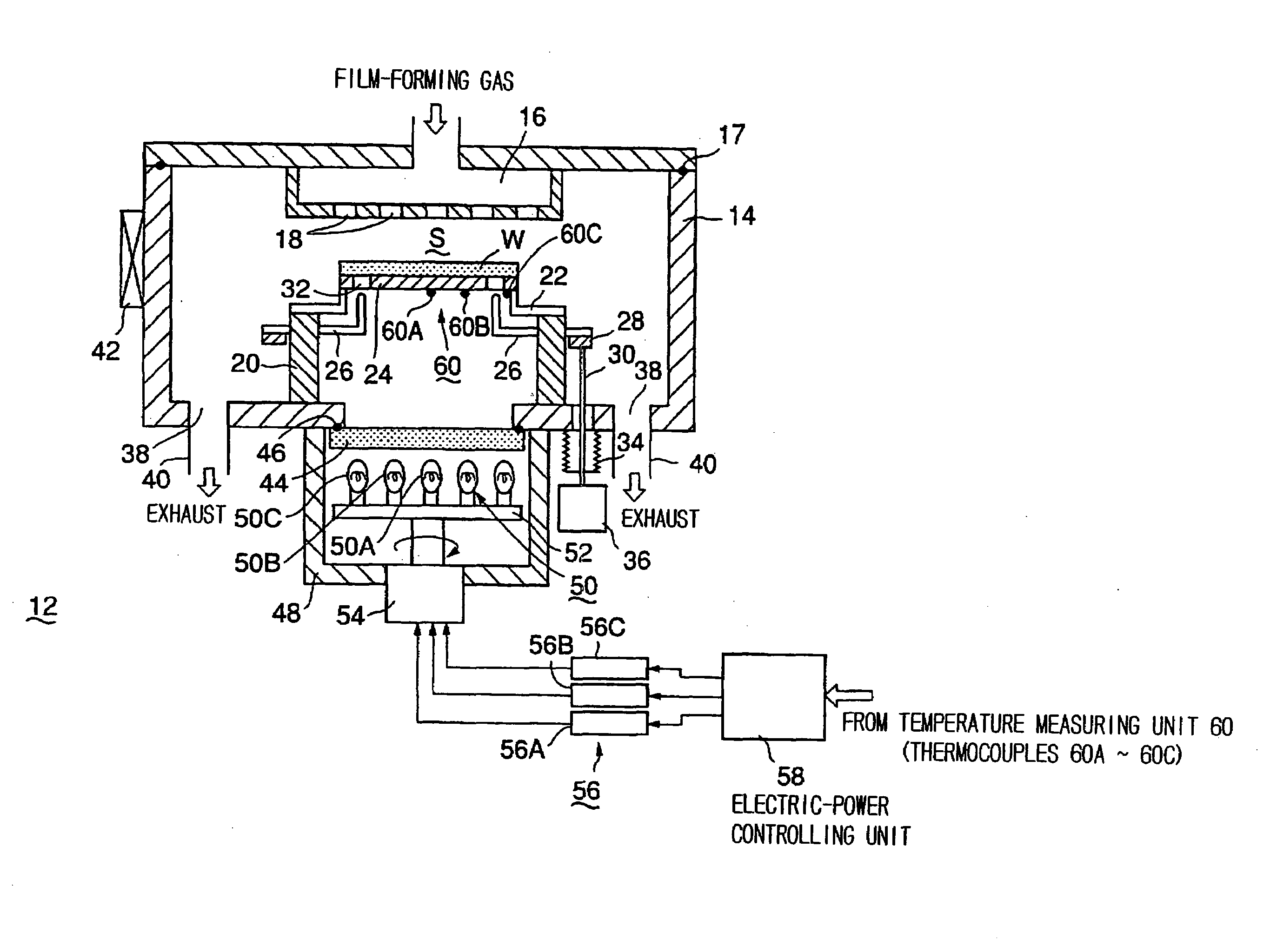
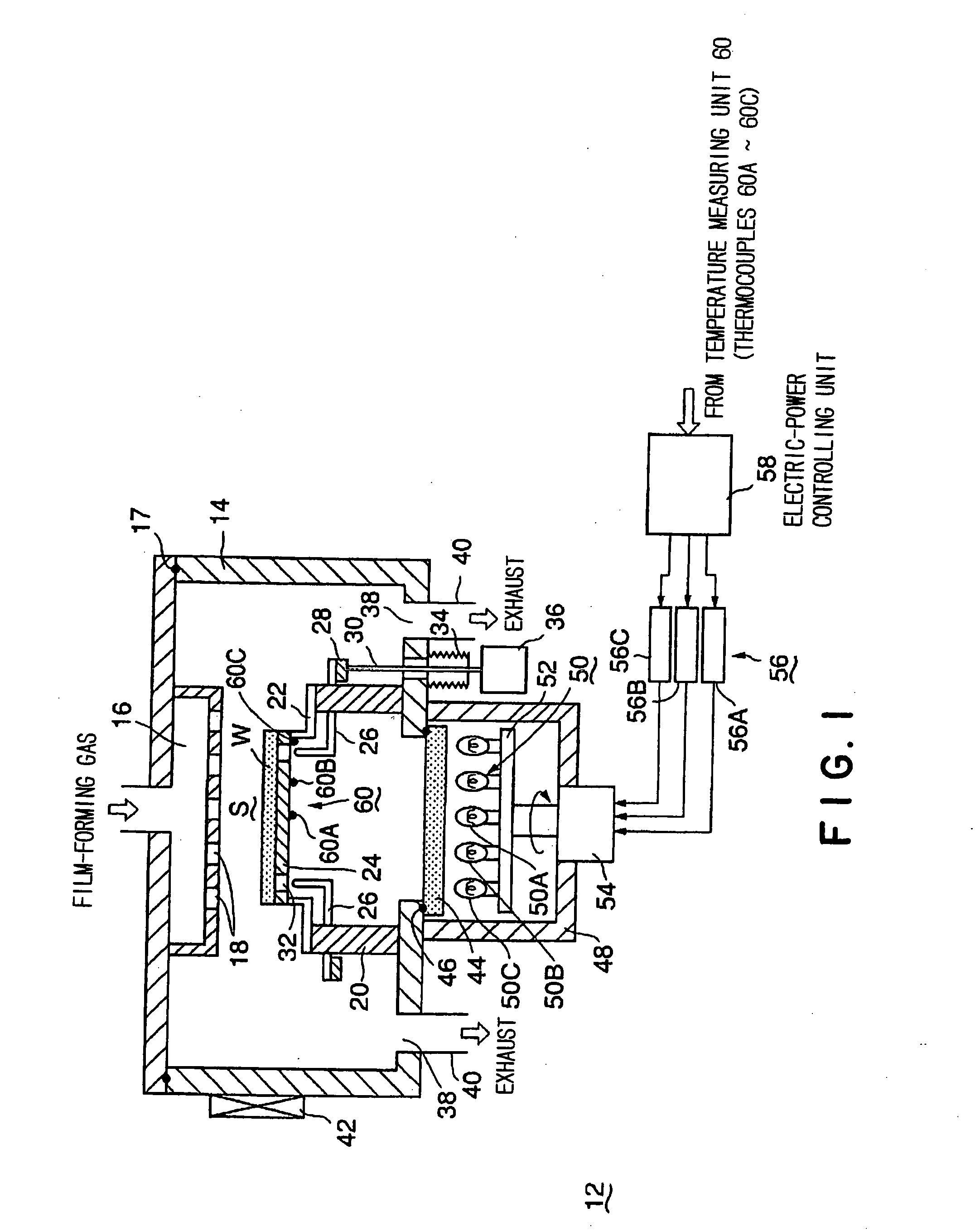
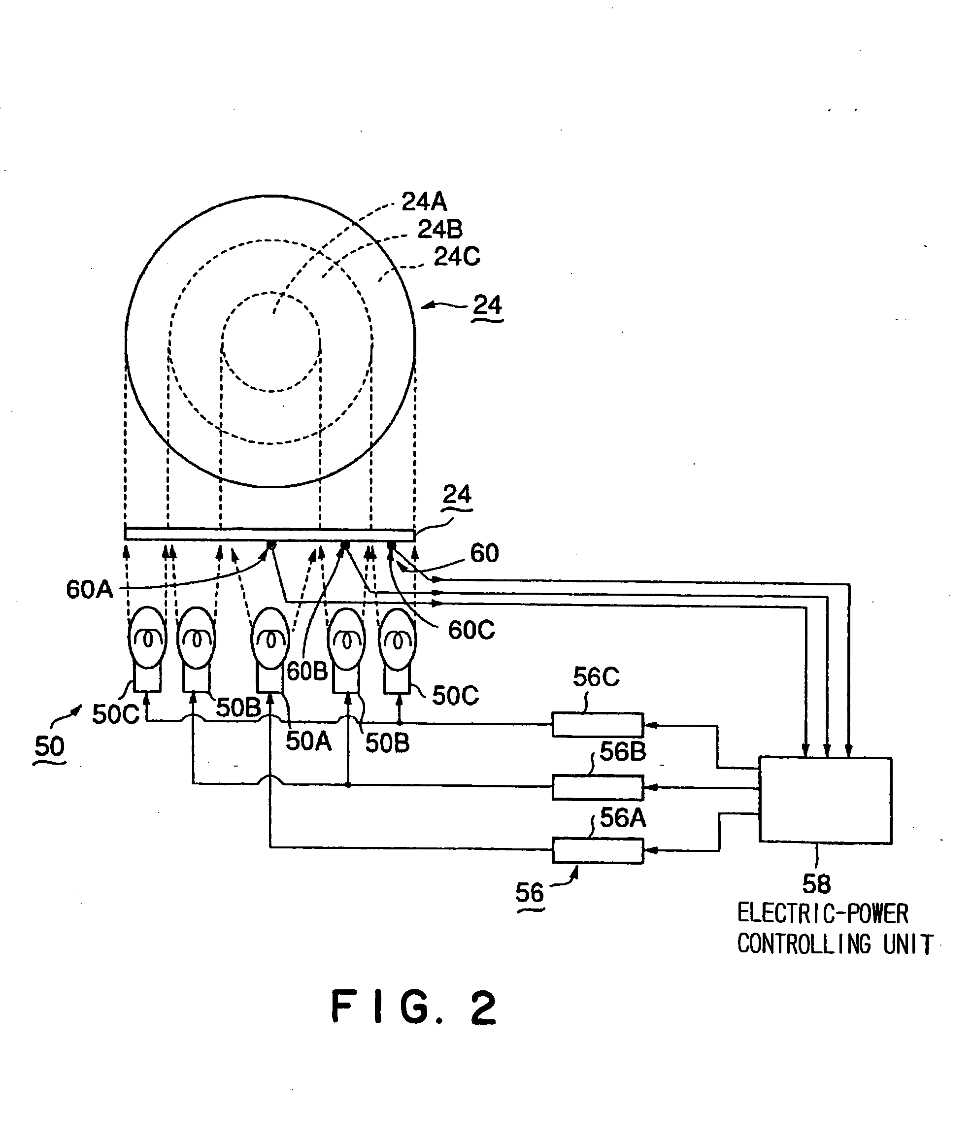
[0047]FIG. 1 is a sectional view showing the embodiment of a processing unit according to the present invention. FIG. 2 is a schematic view showing a control system of a heating unit that heats a stage. FIG. 3 is a schematic view showing an example of shift of a temperature distribution while the object to be processed is heated. Herein, a single wafer film-forming unit is explained as an example of a processing unit.
[0048]As shown in FIG. 1, a film-forming unit 12 has a processing container 14, for example having a substantially cylindrical shape and made of aluminum. A showerhead part 16 is provided at a ceiling part in the processing container 14 via a sealing member 17 such as an O-ring. A large number of gas-jetting holes 18 are provided at a lower surface of the showerhead part 16. Thus, process gases such as various film-forming g...
PUM
 Abstract
Description
Claims
Application Information