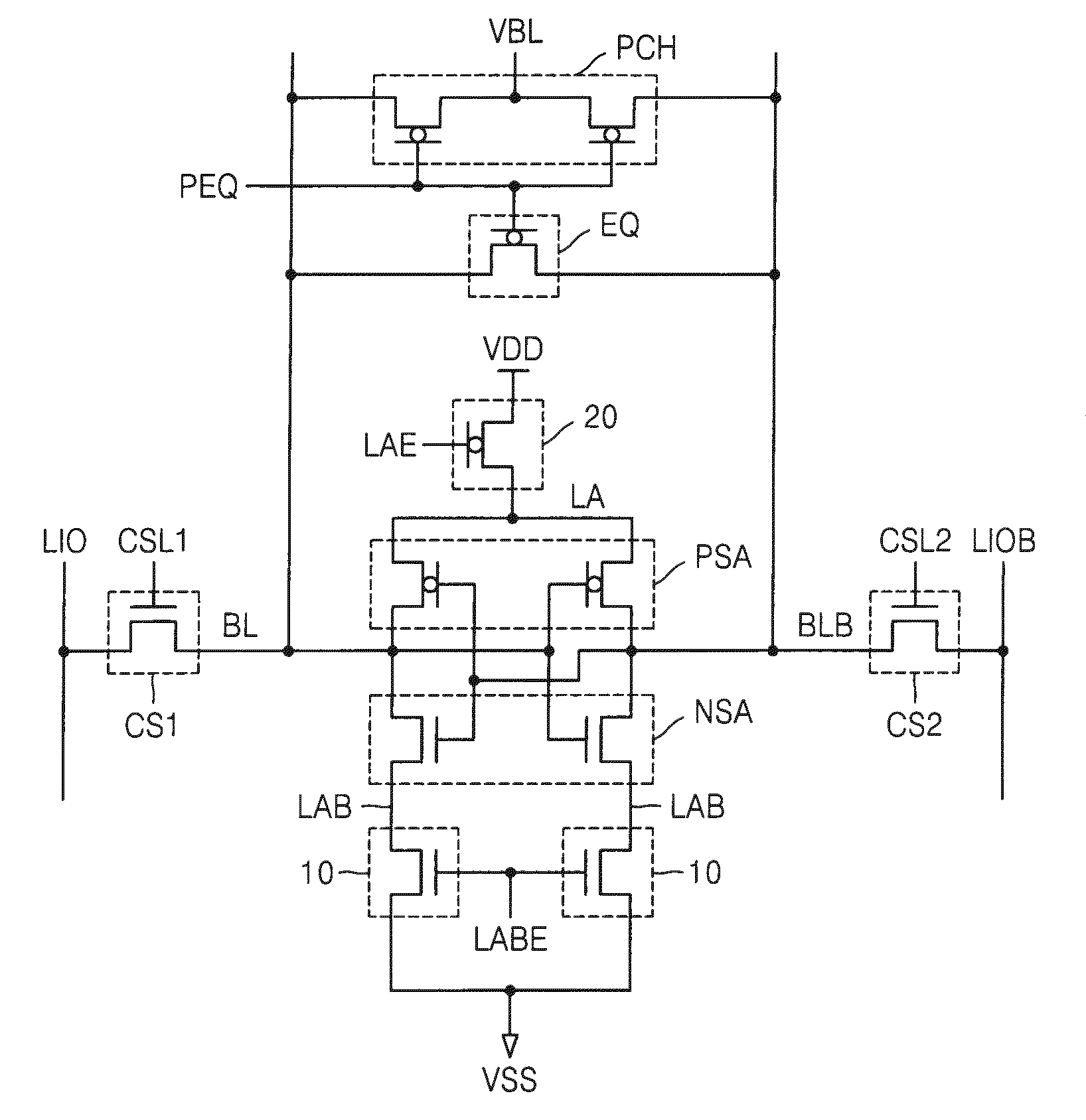
Bit line sense amplifier of semiconductor memory device having open bit line structure

a memory device and bit line sense technology, applied in the field of semiconductor memory devices with open bit line structures, can solve the problems of unstable sensing operation of the bit line sense amplifier with respect to the bit line bl or the complementary bit line blb, and the inability of the nsa driver b>10/b> to stably apply the ground voltage vss, etc., to achieve the effect of stably performing a sensing operation

Active Publication Date: 2009-12-17
SAMSUNG ELECTRONICS CO LTD
View PDF2 Cites 6 Cited by
  • Summary
  • Abstract
  • Description
  • Claims
  • Application Information

AI Technical Summary

Benefits of technology

This configuration enables stable sensing operations for both read and write operations, reducing noise mismatch and enhancing the overall performance of the semiconductor memory device by ensuring consistent voltage application and equal coupling capacitances.

Problems solved by technology

That is, a mismatch occurs between the coupling capacitances of the bit lines and the complementary bit lines.
Therefore, in the semiconductor memory device 5 having the open bit structure, a mismatch in the coupling capacitance may lead to an unstable sensing operation of the bit line sense amplifier with respect to the bit lines BL or the complementary bit lines BLB.
Thus, the NSA driver 10 may not always be capable of stably applying the ground voltage VSS for a stable sensing operation of the NMOS sensing amplifier NSA.
Accordingly, the sensing operation of the bit line sense amplifier for a data write operation or a data read operation may be unstable.

Method used


Image

  • Bit line sense amplifier of semiconductor memory device having open bit line structure
  • Bit line sense amplifier of semiconductor memory device having open bit line structure
  • Bit line sense amplifier of semiconductor memory device having open bit line structure

Examples


Embodiment Construction

[0031]Embodiments provide a bit line sense amplifier of a semiconductor memory device, which is capable of stably performing a sensing operation.

[0032]An aspect of the present invention provides a bit line sense amplifier of a semiconductor memory device with an open bit line structure, the bit line sense amplifier comprising a plurality of sense amplifier blocks including a first sense amplifier and a second sense amplifier, each sensing and amplifying a signal difference between a bit line and a complementary bit line; first voltage drivers applying a power source voltage to the first sense amplifier; and a second voltage driver applying a ground voltage to the second sense amplifier. Each of the first voltage drivers may be disposed for every two or more sense amplifier blocks in a bit line sense amplifier region in which the sense amplifier blocks are arranged. The second voltage driver may be disposed in a conjunction region in which a control circuit is located to control the ...


PUM


Abstract

In an embodiment, a bit line sense amplifier of a semiconductor memory device with an open bit line structure includes sense amplifier blocks, first voltage drivers, and a second voltage driver. The sense amplifier blocks include a first sense amplifier and a second sense amplifier, each sensing and amplifying a signal difference between a bit line and a complementary bit line. The first voltage drivers apply a power source voltage to the first sense amplifier, and the second voltage driver applies a ground voltage to the second sense amplifier. The first voltage drivers are disposed for every two or more sense amplifier blocks in a bit line sense amplifier region in which the sense amplifier blocks are arranged, and the second voltage driver is disposed in a conjunction region in which a control circuit is located to control the sense amplifier blocks. Both capacitive noise and device size are minimized.

Description

CROSS-REFERENCE TO RELATED PATENT APPLICATIONS[0001]This application is a Divisional of U.S. patent application Ser. No. 11 / 834,516, filed on Aug. 6, 2007, now pending, which claims priority under 35 U.S.C. § 119 from Korean Patent Application No. 10-2006-0079526, filed on Aug. 22, 2006, in the Korean Intellectual Property Office, the entire contents of which are hereby incorporated by referenceBACKGROUND[0002]1. Field of the Invention[0003]The present invention relates to a semiconductor memory device, and more particularly, to a semiconductor memory device having an open bit line structure.[0004]2. Description of the Related Art[0005]A bit line sense amplifier of a semiconductor memory device, such as a Dynamic Random Access Memory (DRAM), amplifies a slight signal difference generated in a bit line when a memory cell is accessed and charge sharing occurs between the memory cell and the bit line. Thus, the bit line sense amplifier is a circuit indispensable to the operation of the...

Claims


Application Information

Patent Timeline
Patent Type & AuthorityApplications(United States)
IPC IPC(8): G11C7/02G11C7/00
CPCG11C7/02G11C7/065G11C7/12G11C2207/005G11C11/4091G11C11/4094G11C11/4097G11C7/18G11C7/08G11C2207/002
InventorYANG, HYANG-JAKIM, SU-YEON
OwnerSAMSUNG ELECTRONICS CO LTD