Development verification apparatus for universal chip

a verification apparatus and universal chip technology, applied in the direction of cad circuit design, program control, instruments, etc., can solve the problems of excessive cost of asic production, significant amount of extended interfaces, and inability of the development verification platform and its computation resources to serve as embedded systems, so as to save costs

Inactive Publication Date: 2010-08-19
BEIJING YUDONG TECH DEV
View PDF10 Cites 25 Cited by
  • Summary
  • Abstract
  • Description
  • Claims
  • Application Information

AI Technical Summary

Benefits of technology

[0012]The present invention provide a development verification apparatus for universal chip, whose cascade structure connected with the universal inte

Problems solved by technology

It is very expensive to produce the ASIC, so the verification must be fully carried out by the FPGA to eliminate all potential problems before entering the ASIC producing stage.
1. The design capacities vary from different object chips, and the scale of a FPGA should be selectable for the purpose of cost reduction.
2. The development verification platform is expected to posses not only a FPGA of proper capacity but external devices of particular functions to carry out auxiliary design.
3. As for the design of the intellectual property core or the SOC that needs to work cooper

Method used


Image

  • Development verification apparatus for universal chip
  • Development verification apparatus for universal chip
  • Development verification apparatus for universal chip

Examples


Embodiment Construction

[0051]It is to be understood that other embodiments may be utilized and structural changes may be made without departing from the scope of the present invention. Also, it is to be understood that the phraseology and terminology used herein are for the purpose of description and should not be regarded as limiting. The use of “including,”“comprising,” or “having” and variations thereof herein is meant to encompass the items listed thereafter and equivalents thereof as well as additional items. Unless limited otherwise, the terms “connected,” and “coupled,” and variations thereof herein are used broadly and encompass direct and indirect connections, couplings, and mountings.

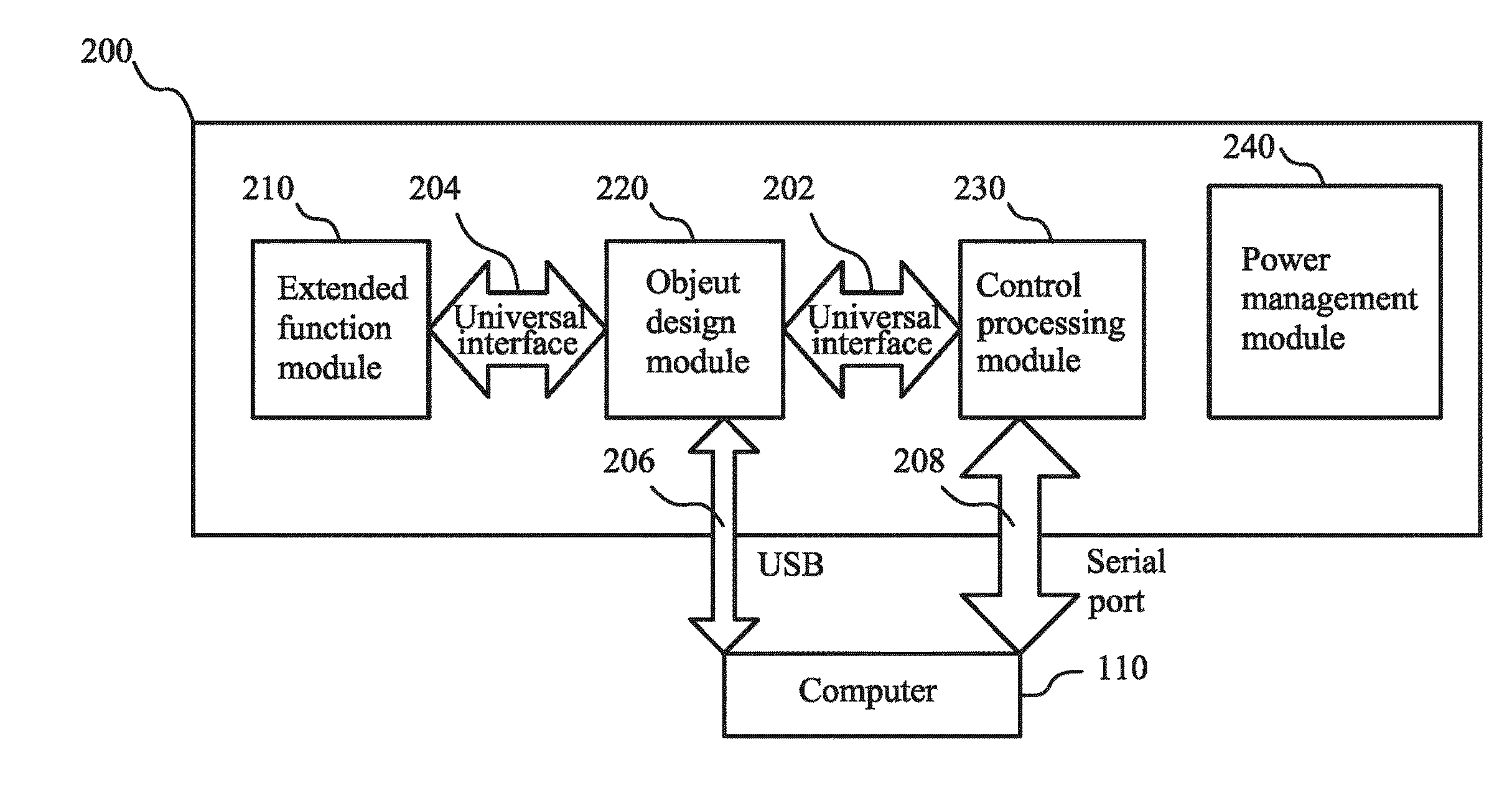
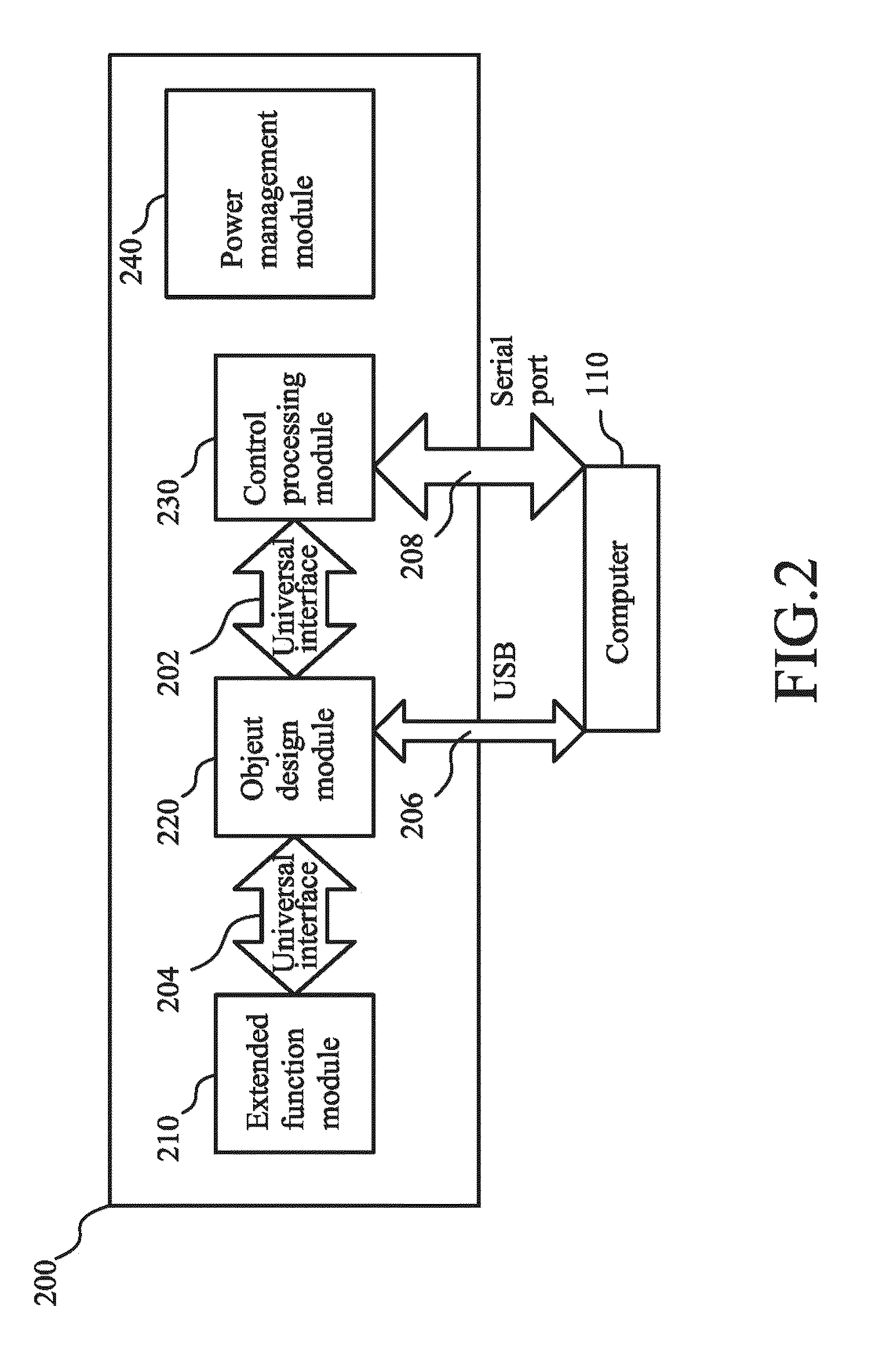
[0052]The structural diagram of a development verification apparatus for universal chip is shown in FIG. 2. The development verification apparatus includes: an object design module 220 storing and executing an object code of the chip to be verified; a control processing module 230 executing the control program and e...


PUM


Abstract

A development verification apparatus for verification of universal chips, including an object design module for storing and executing the object code of the chip to be verified, a control processing module for executing the control program etc. of the user of the development verification apparatus, a power management module for managing the power and charging the battery, and an extended function module for implementing developing function in various fields.

Description

BACKGROUND OF THE INVENTION[0001]1. Field of the Invention[0002]The present invention relates to a development verification apparatus for universal chip, and more particularly relates to a universal, high speed, elastic and extendable development verification platform for chip of the integrated circuit, which belongs to the field of the chip design.[0003]2. Description of the Prior Art[0004]The general way to develop a chip is to complete the initial objective design on the field programmable gate array (FPGA), and then convert it into an application specific integrated circuit (ASIC) after verification, test and correction processes until the performance satisfies the design requirements. It is very expensive to produce the ASIC, so the verification must be fully carried out by the FPGA to eliminate all potential problems before entering the ASIC producing stage. Therefore, a stable and powerful FPGA development verification apparatus is needed to support the object design and ensu...

Claims


Application Information

Patent Timeline
IPC IPC(8): G06F17/50
CPCG06F17/5022G06F30/33
Inventor HU, BOZHAO, ZHENFENGYU, DAYONG
Owner BEIJING YUDONG TECH DEV
Why Eureka
Try Eureka