Electromagnetic Interference Shielding for Compact Electronic Devices

a technology of electronic devices and shielding, applied in the association of printed circuit non-printed electric components, manufacturing tools, electrical apparatus contruction details, etc., can solve the problems of reducing the effective performance of enclosures, affecting the efficiency of substrate space, and affecting the efficiency of electrical devices. , to achieve the effect of wide electrical components, efficient utilization of substrate space, and increased substrate width

Inactive Publication Date: 2010-09-30
APPLE INC
View PDF30 Cites 42 Cited by
  • Summary
  • Abstract
  • Description
  • Claims
  • Application Information

AI Technical Summary

Benefits of technology

[0005]The invention pertains to improved approaches for providing electromagnetic interference (EMI) shielding to one or more electrical components within a housing of a portable electronic device. According to one aspect of certain embodiments of the invention, an electromagnetic shield can be attached to one or more edges of a substrate (e.g., printed circuit board) provided within a housing of a portable electronic device. Advantageously, this allows the substrate space to be efficiently utilized such that relatively wide electrical components can be provided on the substrate without having to further increase the width of the substrate to provide space for an EMI shielding structure and its attachment to the substrate. The housing of the portable electronic device can be compact, such as a low profile housing.

Problems solved by technology

Electromagnetic interference (EMI) is an unwanted disturbance that affects an electrical device due to either electromagnetic conduction or electromagnetic radiation emitted from an external source.
The disturbance may interrupt, obstruct, or otherwise degrade or limit the effective performance of the electrical device.
Any holes in the shield must be significantly smaller than the wavelength of the radiation that is being kept out, or the enclosure will not be effective.
Unfortunately, however, as compact portable electronic devices become increasingly more compact, the availability of space within a housing for a compact electronic device becomes more limited.
Accordingly, given the constrained geometries and tight tolerances of compact portable electronic devices, such as handheld portable electronic devices, it is increasingly difficult to provide EMI shielding without causing a significant area increase penalty to housing designs for compact electronic devices.

Method used


Image

  • Electromagnetic Interference Shielding for Compact Electronic Devices
  • Electromagnetic Interference Shielding for Compact Electronic Devices
  • Electromagnetic Interference Shielding for Compact Electronic Devices

Examples


Embodiment Construction

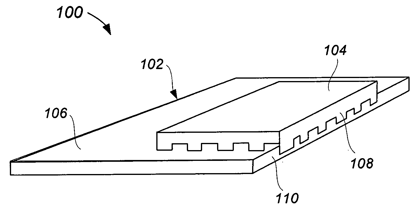
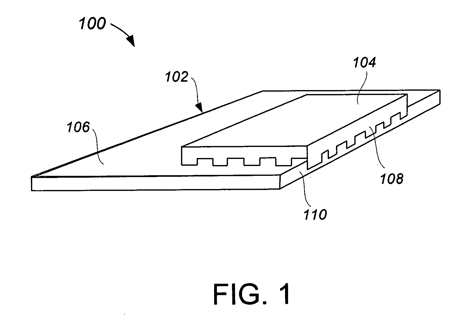
[0023]The invention pertains to improved approaches for providing electromagnetic interference shielding to one or more electrical components within a housing of a portable electronic device. According to one aspect of certain embodiments of the invention, an electromagnetic shield can be attached to one or more edges of a substrate (e.g., printed circuit board) provided within a housing of a portable electronic device. Advantageously, this allows the substrate space to be efficiently utilized such that relatively wide electrical components can be provided on the substrate without having to further increase the width of the substrate to provide space for an EMI shielding structure and its attachment to the substrate.

[0024]The housing of the portable electronic device can be compact, such as a low profile housing. The portable electronic device can pertain to a portable digital media player, a mobile telephone, personal digital assistant, handheld computing devices, etc.

[0025]Embodim...


PUM

PropertyMeasurementUnit
thicknessaaaaaaaaaa
conductiveaaaaaaaaaa
electromagnetic interferenceaaaaaaaaaa

Abstract

Improved approaches for providing electromagnetic interference shielding to one or more electrical components within a housing of a portable electronic device are disclosed. According to one aspect of certain embodiments, an electromagnetic shield can be attached to one or more edges of a substrate (e.g., printed circuit board) provided within a housing of a portable electronic device. Advantageously, this allows the substrate space to be efficiently utilized such that relatively wide electrical components can be provided on the substrate without having to further increase the width of the substrate to provide space for an EMI shielding structure and its attachment to the substrate. The housing of the portable electronic device can be compact, such as a low profile housing.

Description

BACKGROUND OF THE INVENTION[0001]Electromagnetic interference (EMI) is an unwanted disturbance that affects an electrical device due to either electromagnetic conduction or electromagnetic radiation emitted from an external source. The disturbance may interrupt, obstruct, or otherwise degrade or limit the effective performance of the electrical device. EMI can also be referred to as radio frequency interference (RFI). The Federal Communications Commission (FCC) has developed standards for EMI immunity for consumer electronic devices.[0002]Electromagnetic shielding can be used to limit the penetration of electromagnetic fields into a space by blocking them with a barrier made of conductive material. Typically, the barrier is implemented as an enclosure that separates electrical devices from the outside world. Electromagnetic shielding used to block radio frequency electromagnetic radiation is also known as RF shielding. Typical materials used for electromagnetic shielding include she...

Claims


Application Information

Patent Timeline
Patent Type & Authority Applications(United States)
IPC IPC(8): H05K7/00H05K9/00H05K13/04
CPCH05K9/0026Y10T29/5313H05K9/0028
Inventor DINH, RICHARD HUNG MINHJUST, ANDREWPYPER, DENNISFIENNES, HUGOMYERS, SCOTTWANG, ERIKDIMPFLMAIER, RON
Owner APPLE INC
Why Eureka
Try Eureka