

Semiconductor memory device and operating method thereof
a memory device and semiconductor technology, applied in the field of semiconductor memory devices and an operating method thereof, can solve the problems of deteriorating characteristics of memory cells, difficult to supplement the edge region with boron, and interference phenomena between adjacent memory cells
- Summary
- Abstract
- Description
- Claims
- Application Information
AI Technical Summary
Benefits of technology
Problems solved by technology
Method used
Image



Examples
first embodiment
[0055]Table 1 shows voltages supplied according to this disclosure.
TABLE 1ProgramProgramverifyReadErase verifyVp_wellNegativeNegativeNegativeNegativevoltagevoltagevoltagevoltageVn_wellPositivePositivePositivePositivevoltagevoltagevoltagevoltage
[0056]As shown Table 1, when the program, program verify, the read operation, and the erase verify operation are performed, the voltage Vp_well supplied to the P well is the negative voltage, and the voltage Vn_well supplied to the N well is the positive voltage.
[0057]For example, the program operation is described in detail below.
[0058]FIG. 5 is a flowchart illustrating a program operation.
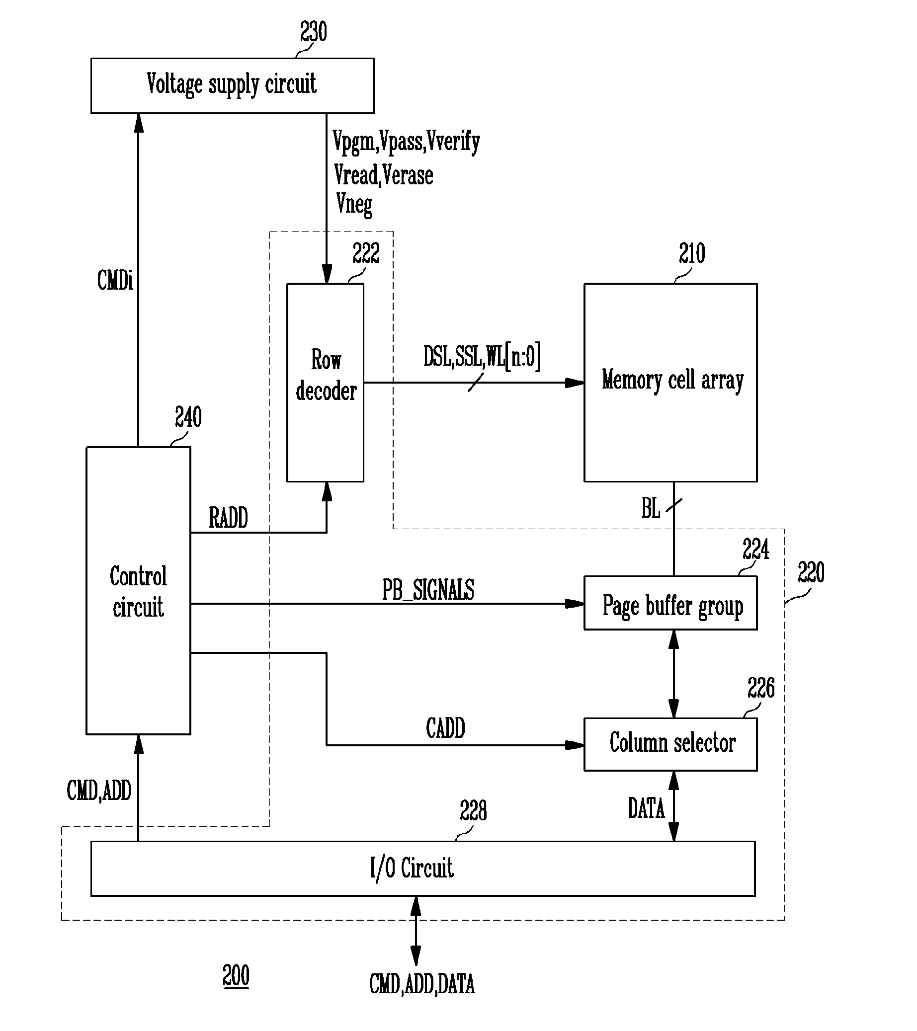
[0059]Referring to FIG. 5, for the program operation, a program command and an address are inputted to the semiconductor memory device, and data to be programmed is then inputted thereto at steps S510 and S520.
[0060]The program command and the address are transferred to the control circuit 240 via the peripheral circuit 220. The data to be programmed is sto...
second embodiment
[0086]Table 2 shows voltages supplied according to this disclosure.
TABLE 2ProgramProgramverifyReadErase verifyVp_wellNegativeNegativeNegativeNegativevoltagevoltagevoltagevoltageVn_well0 V0 V0 V0 V
[0087]Referring to Table 2, when program, program verify, read, and erase verify operations are performed, negative voltage is supplied to the P well and 0 V is supplied to the N well.
[0088]That is, when step S530 of FIG. 5 is performed, the program voltage Vpgm is supplied to the selected word line, the pass voltage is supplied to the unselected word lines, the negative voltage is supplied to the P well, and 0 V is supplied to the N well.
[0089]The voltages start being supplied to the P well and the N well when voltage supplied to the bit lines is set for the program operation.
[0090]When the program verify operation of step S540 is performed, negative voltage is supplied to the P well and 0 V is supplied to the N well.
[0091]Furthermore, in the read operation and the erase verify operation, ...
PUM
 Abstract
Description
Claims
Application Information