
Optoelectronic Semiconductor Body and Method for Producing an Optoelectronic Semiconductor Body
a technology of optoelectronic semiconductor and semiconductor body, which is applied in the direction of semiconductor devices, electrical equipment, optical wave guidance, etc., can solve the problems of semiconductor body deflection and/or cracks in epitaxial layer sequence, and achieve the reduction of epitaxial layer sequence cracks and/or tension between substrate and epitaxial layer sequen
- Summary
- Abstract
- Description
- Claims
- Application Information
AI Technical Summary
Benefits of technology
Problems solved by technology
Method used
Image

Examples
Embodiment Construction
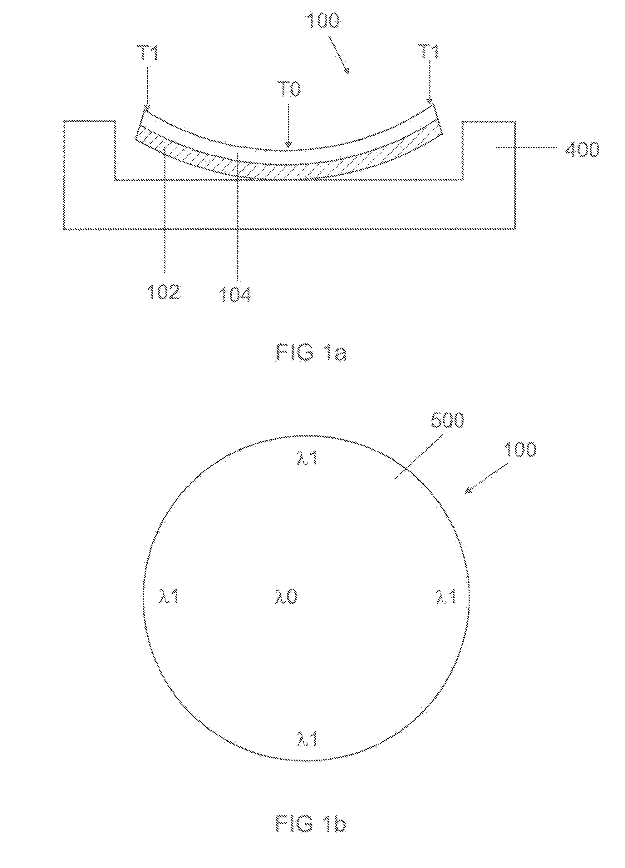
[0062]FIG. 1a shows a sectional view of a known optoelectronic semiconductor body 100 having a deflection. A tensioned layer 104 is grown on the substrate 102. The tension between the substrate 102 and the tensioned layer 104 is the cause of the deflection. The semiconductor body 100 is arranged on a carrier 400 in epitaxy equipment (not shown). Because of the deflection of the semiconductor body 100, the semiconductor body 100 does not rest completely on the carrier 400. An inhomogeneous temperature profile thus results over the extension of the semiconductor body 100 in parallel to the carrier 400. The semiconductor body 100 has a temperature T0 in the center which is higher than a temperature T1 at the edge.
[0063]FIG. 1b shows a top view of a known optoelectronic semiconductor body 100. The semiconductor body has a disk shape. The semiconductor body is completely processed, i.e., all epitaxial layers have been grown on the substrate 102. The entirety of the epitaxial layers is pr...
PUM
 Abstract
Description
Claims
Application Information