Optoelectronic semiconductor body and method for producing an optoelectronic semiconductor body

a technology of optoelectronic semiconductor and semiconductor body, which is applied in the direction of semiconductor devices, electrical equipment, optical wave guidance, etc., can solve the problems of semiconductor body deflection and/or cracks in epitaxial layer sequence, and achieve the reduction of epitaxial layer sequence cracks and/or tension between substrate and epitaxial layer sequen

Active Publication Date: 2016-10-25
OSRAM OLED
View PDF24 Cites 0 Cited by
  • Summary
  • Abstract
  • Description
  • Claims
  • Application Information

AI Technical Summary

Benefits of technology

[0004]Embodiments of the invention specify an optoelectronic semiconductor body, in which the tension between substrate and epitaxial layer sequence and / or the cracking in the epitaxial layer sequence is reduced.
[0005]Various embodiments of an optoelectronic semiconductor body have a tensioned layer, which was applied in a first epitaxy step to a substrate. The tensioned layer has at least one recess formed vertically in the tensioned layer. In a second epitaxy step, a further layer was applied to the tensioned layer, which fills up the at least one recess and at least regionally covers the tensioned layer. This arrangement ensures that the tension between substrate and epitaxial layer sequence and / or the cracking in the epitaxial layer sequence is reduced.
[0006]The tension occurs because the “natural” lattice constants of the substrate and of the tensioned layer are different from one another. “Natural” means in the present document that the value of the lattice constant was respectively determined on an isolated system. In other words, the values of the lattice constants apply for layers in the non-tensioned state, i.e., for layers which are not in contact with one another. The term “lattice constant” always means “natural lattice constant” hereafter. In addition, the term lattice constant in the present case designates the value of the lattice constant parallel to the growth surface of the epitaxial layers. The greater the deviation of the lattice constants from layers which are epitaxially grown directly on one another, the stronger the tension between these layers in general.

Problems solved by technology

Such tensions can result in deflection of the semiconductor body and / or cracks in the epitaxial layer sequence.

Method used


Image

  • Optoelectronic semiconductor body and method for producing an optoelectronic semiconductor body
  • Optoelectronic semiconductor body and method for producing an optoelectronic semiconductor body
  • Optoelectronic semiconductor body and method for producing an optoelectronic semiconductor body

Examples


Embodiment Construction

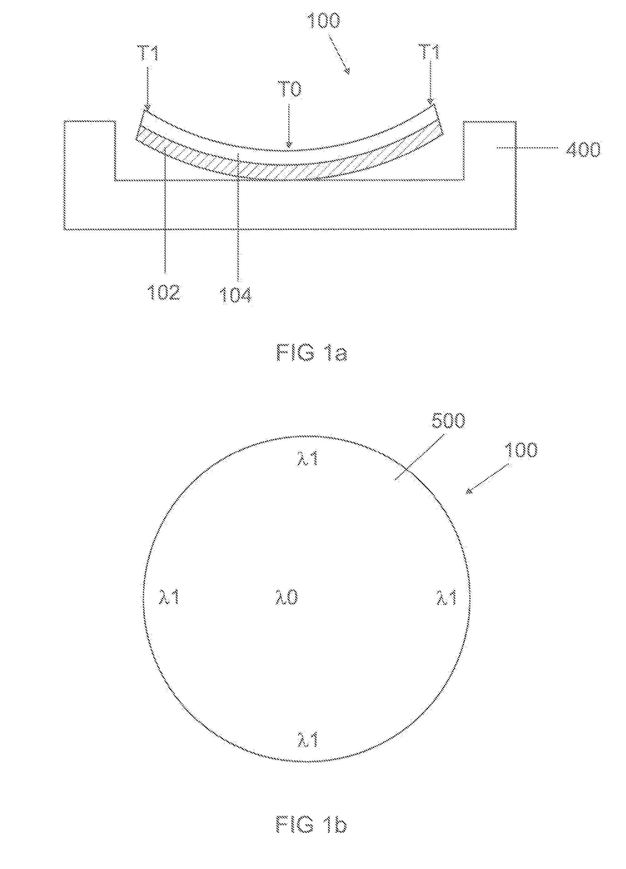
[0062]FIG. 1a shows a sectional view of a known optoelectronic semiconductor body 100 having a deflection. A tensioned layer 104 is grown on the substrate 102. The tension between the substrate 102 and the tensioned layer 104 is the cause of the deflection. The semiconductor body 100 is arranged on a carrier 400 in epitaxy equipment (not shown). Because of the deflection of the semiconductor body 100, the semiconductor body 100 does not rest completely on the carrier 400. An inhomogeneous temperature profile thus results over the extension of the semiconductor body 100 in parallel to the carrier 400. The semiconductor body 100 has a temperature T0 in the center which is higher than a temperature T1 at the edge.

[0063]FIG. 1b shows a top view of a known optoelectronic semiconductor body 100. The semiconductor body has a disk shape. The semiconductor body is completely processed, i.e., all epitaxial layers have been grown on the substrate 102. The entirety of the epitaxial layers is pr...


PUM


Abstract

An optoelectronic semiconductor body has a substrate that includes a strained layer that is applied to the substrate in a first epitaxy step. The strained layer includes at least one recess formed vertically in the strained layer. In a second epitaxy step, a further layer applied to the strained layer. The further layer fills the at least one recess and covers the strained layer at least in some areas.

Description

[0001]This patent application is a national phase filing under section 371 of PCT / EP2012 / 058969, filed May 15, 2012, which claims the priority of German patent application 10 2011 077 542.0, filed Jun. 15, 2011, each of which is incorporated herein by reference in its entirety.TECHNICAL FIELD[0002]The present invention relates to an optoelectronic semiconductor body and a method for producing an optoelectronic semiconductor body.BACKGROUND[0003]Optoelectronic semiconductor bodies typically have an epitaxial layer sequence comprising an active layer suitable for generating electromagnetic radiation. The entirety of the epitaxially grown semiconductor layers is designated as an epitaxial layer sequence. Such an epitaxial layer sequence can be deposited by means of epitaxy on a substrate. Mechanical tensions can occur between the epitaxial layer sequence and the substrate. Such tensions can result in deflection of the semiconductor body and / or cracks in the epitaxial layer sequence. Th...

Claims


Application Information

Patent Timeline
Patent Type & Authority Patents(United States)
IPC IPC(8): H01L29/49H01S5/22H01L21/02H01L29/20H01L29/205
CPCH01S5/22H01L21/0242H01L21/0254H01L21/02381H01L21/02389H01L21/02458H01L21/02507H01L21/02576H01L21/02609H01L21/02647H01L29/2003H01L29/205H01L31/0216H01L31/0236H01L31/02366H01L31/18
Inventor AVRAMESCU, ADRIAN STEFANPIETZONKA, INESDINI, DIMITRI
Owner OSRAM OLED
Why Eureka
Try Eureka