

Display device and electronic device
Active Publication Date: 2014-05-29
SEMICON ENERGY LAB CO LTD
View PDF4 Cites 16 Cited by
- Summary
- Abstract
- Description
- Claims
- Application Information
AI Technical Summary
Benefits of technology
The invention improves the reliability of a display device.
Problems solved by technology
If a surge voltage due to static electricity or the like is applied to a display device, an element is broken to produce abnormal display.
Method used
View moreImage
Smart ImageViewing Examples

Examples
embodiment 1 (
1. Embodiment 1 (Basic structure relating to one embodiment of the present invention)
embodiment 2 (
2. Embodiment 2 (Components of display device)
3. Embodiment 3 (Method for manufacturing display device)
embodiment 4 (
4. Embodiment 4 (Configuration of pixel circuit)
5. Embodiment 5 (Structures of pixel portion)
Login to View More PUM
 Abstract
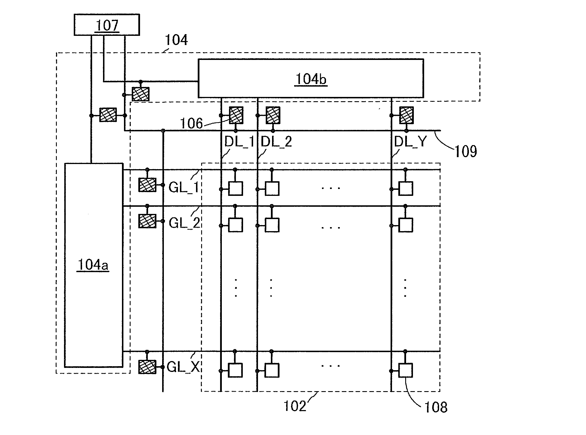
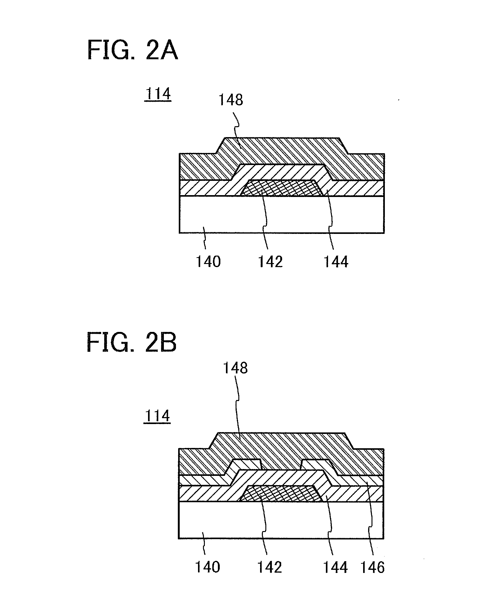
To provide a novel display device. The display device includes a pixel portion, a driver circuit portion that is provided outside the pixel portion, and a protection circuit that is electrically connected to one of or both the pixel portion and the driver circuit portion and includes a pair of electrodes. The pixel portion includes pixel electrodes arranged in a matrix and transistors electrically connected to the pixel electrodes. The transistor includes a first insulating layer containing nitrogen and silicon, and a second insulating layer containing oxygen, nitrogen, and silicon. The protection circuit includes the first insulating layer between the pair of electrodes.
Description
BACKGROUND OF THE INVENTION[0001]1. Field of the Invention[0002]The present invention relates to an object, a method, a production method, a process, a machine, a manufacture, and a composition (a composition of matter). In particular, the present invention relates to a semiconductor device, a display device, a light-emitting device, an electronic device, a driving method thereof, or a manufacturing method thereof. In particular, the present invention relates to a semiconductor device, a display device, an electronic device or a light-emitting device each including an oxide semiconductor.[0003]Note that the term “display device” means a device including a display element. In addition, the display device also includes a driver circuit for driving a plurality of pixels, and the like. Further, the display device includes a control circuit, a power supply circuit, a signal generation circuit, or the like formed over another substrate.[0004]2. Description of the Related Art[0005]For disp...
Claims
Login to View More Application Information
Patent Timeline
 IPC IPC(8): H01L27/12
CPCH01L27/124H01L27/1225H01L27/1248H01L27/0296H10K59/123H10K59/131H10K59/1201G09F9/30G09G3/20G06F3/041H01L29/7869H04N5/44G09G2300/0426H01L27/1244
InventorYAMAZAKI, SHUNPEIKIMURA, HAJIMEMIYAKE, HIROYUKIKOYAMA, JUN
OwnerSEMICON ENERGY LAB CO LTD