
Array substrate manufacturing method, array substrate formed thereby and liquid crystal display apparatus
a technology of array substrates and manufacturing methods, applied in the field of array substrate manufacturing methods and array substrates, can solve the problems of reducing the aperture rate of pixel units, increasing the power consumption lowering the overall brightness level of the liquid crystal display apparatus, so as to achieve the effect of lowering the aperture ra
- Summary
- Abstract
- Description
- Claims
- Application Information
AI Technical Summary
Benefits of technology
Problems solved by technology
Method used
Image

Examples
Embodiment Construction
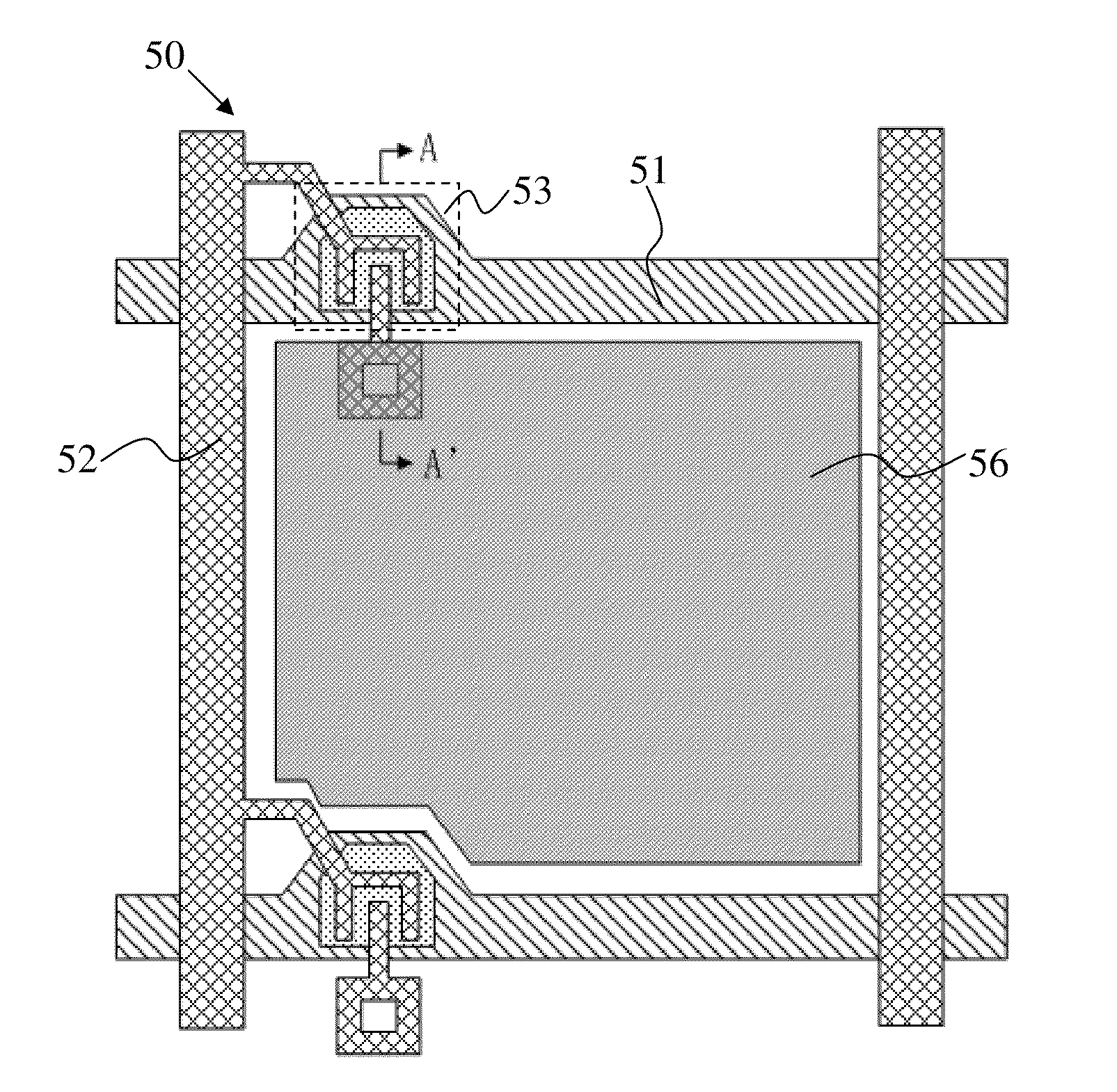
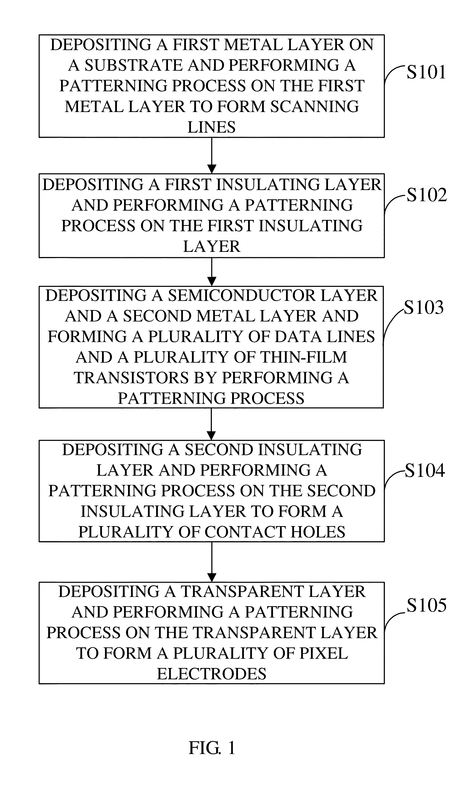
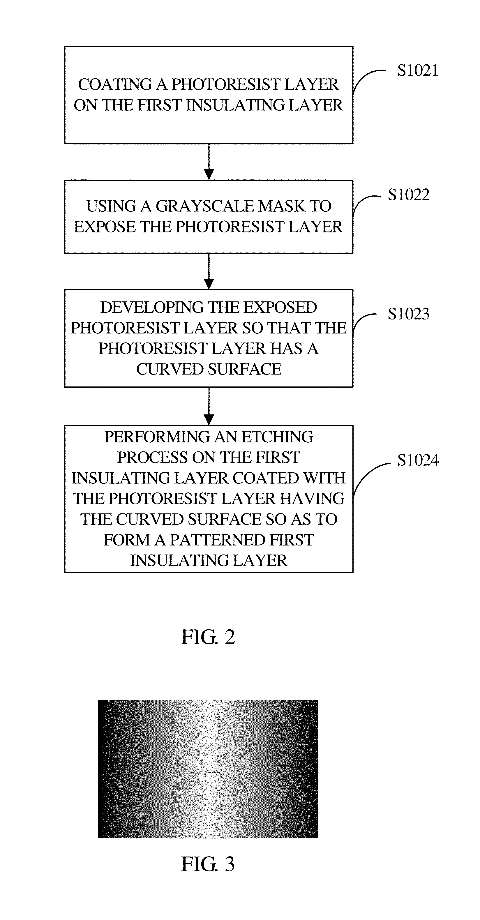
[0063]The following description of each embodiment is referring to the accompanying drawings so as to illustrate practicable specific embodiments in accordance with the present invention. The directional terms described in the present invention, such as upper, lower, front, rear, left, right, inner, outer, side, etc., are only directions referring to the accompanying drawings, so that the used directional terms are used to describe and understand the present invention, but the present invention is not limited thereto.
[0064]A preferred embodiment of the present invention provides an array substrate manufacturing method. FIG. 1 is a flow chart of an array substrate manufacturing method according to a preferred embodiment of the present invention. The array substrate manufacturing method of the preferred embodiment comprises steps of:[0065]Step S101: depositing a first metal layer on a substrate and performing a patterning process on the first metal layer to form a plurality of scannin...
PUM
| Property | Measurement | Unit |
|---|---|---|
| thickness | aaaaa | aaaaa |
| transparent | aaaaa | aaaaa |
| grayscale | aaaaa | aaaaa |
Abstract
Description
Claims
Application Information