Array substrate manufacturing method, array substrate formed thereby and liquid crystal display apparatus

a technology of array substrates and manufacturing methods, applied in the field of array substrate manufacturing methods and array substrates, can solve the problems of reducing the aperture rate of pixel units, increasing the power consumption lowering the overall brightness level of the liquid crystal display apparatus, so as to achieve the effect of lowering the aperture ra

Active Publication Date: 2017-08-15
TCL CHINA STAR OPTOELECTRONICS TECH CO LTD
View PDF9 Cites 0 Cited by
  • Summary
  • Abstract
  • Description
  • Claims
  • Application Information

AI Technical Summary

Benefits of technology

[0010]An object of the present invention is to provide an array substrate manufacturing method, an array substrate formed by the method, and a liquid crystal apparatus having the same so as to solve a technical problem where the image displayed by conventional liquid crystal devices has an uneven brightness level or the conventional liquid crystal devices have a lower aperture rate.
[0056]Compared with the conventional liquid crystal display apparatus, the present invention uses a first insulating layer with different thicknesses so that the liquid crystal display apparatus can display images with an even brightness level, thereby solving the technical problem where the image displayed by conventional liquid crystal devices has an uneven brightness level or the conventional liquid crystal devices have a lower aperture rate.

Problems solved by technology

However, increasing the line width of the scanning lines will also reduce the aperture rate of pixel units.
However, this will lower the overall brightness level of the liquid crystal display apparatus, which needs to be further enhanced by increasing the power of a backlight module that will raise the power consumption of the liquid crystal display apparatus.

Method used


Image

  • Array substrate manufacturing method, array substrate formed thereby and liquid crystal display apparatus
  • Array substrate manufacturing method, array substrate formed thereby and liquid crystal display apparatus
  • Array substrate manufacturing method, array substrate formed thereby and liquid crystal display apparatus

Examples


Embodiment Construction

[0063]The following description of each embodiment is referring to the accompanying drawings so as to illustrate practicable specific embodiments in accordance with the present invention. The directional terms described in the present invention, such as upper, lower, front, rear, left, right, inner, outer, side, etc., are only directions referring to the accompanying drawings, so that the used directional terms are used to describe and understand the present invention, but the present invention is not limited thereto.

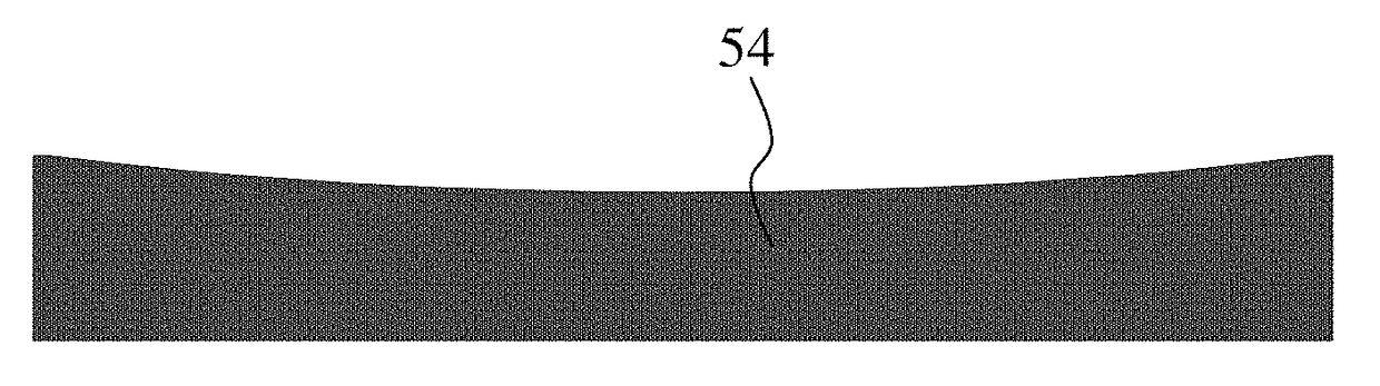
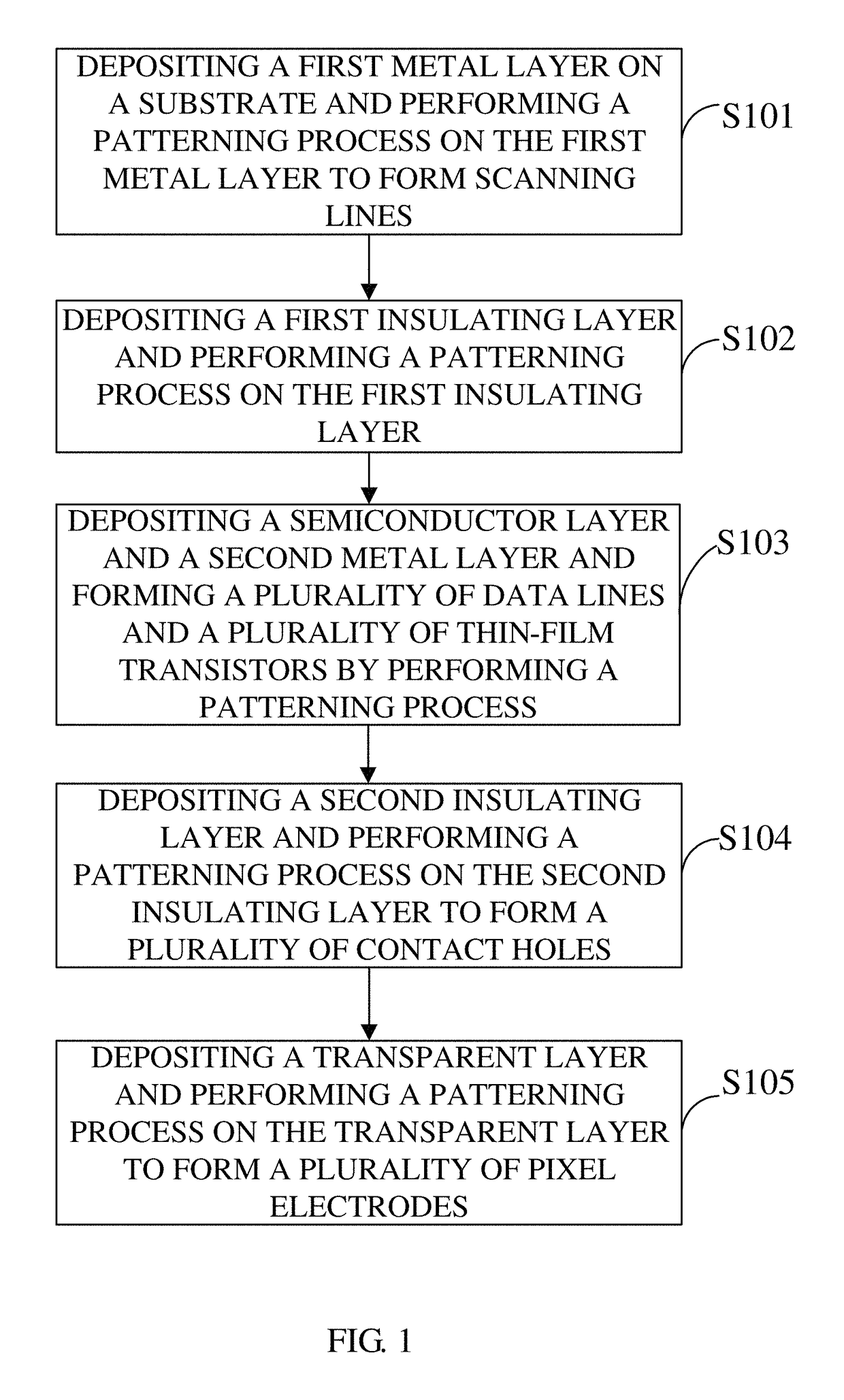
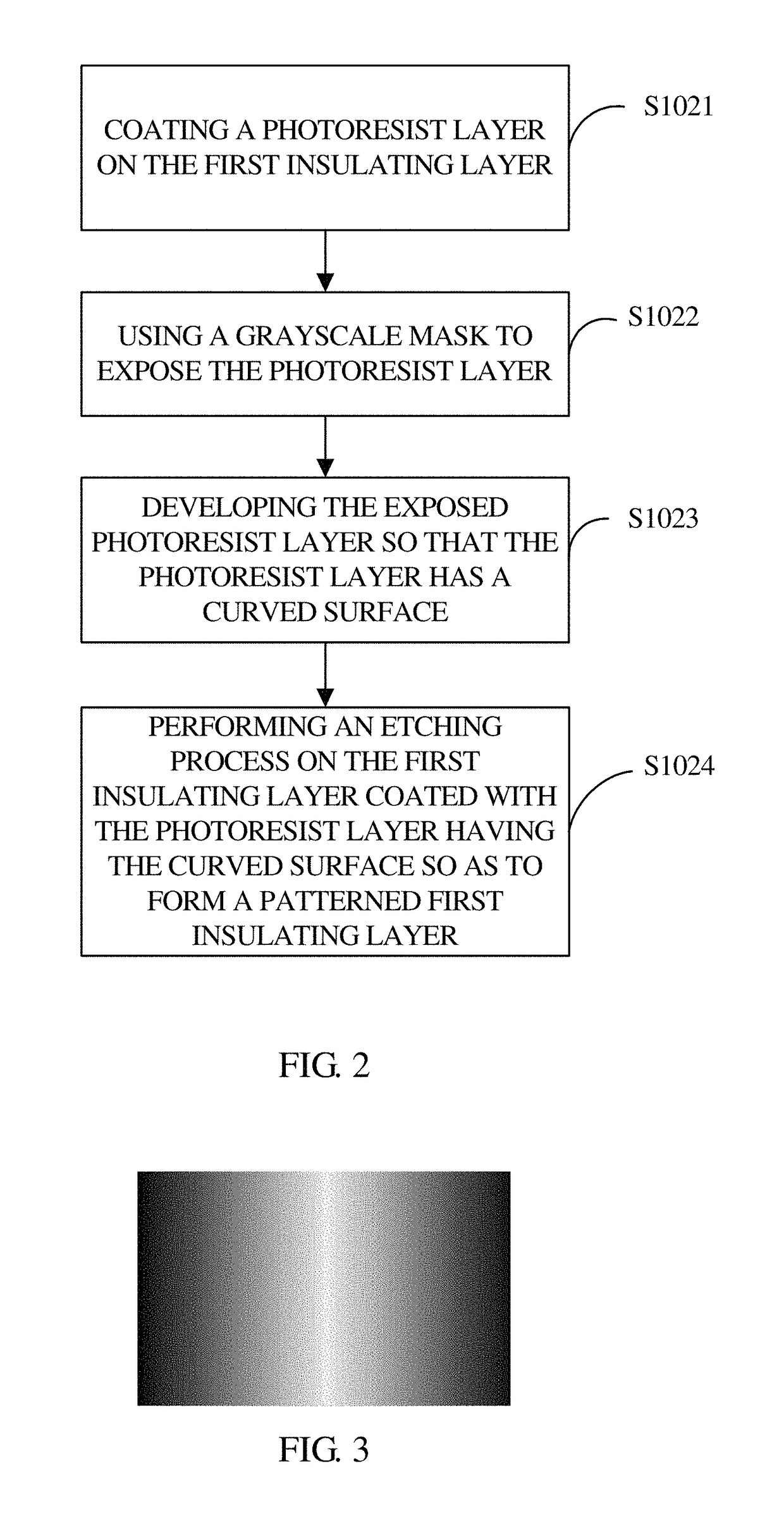
[0064]A preferred embodiment of the present invention provides an array substrate manufacturing method. FIG. 1 is a flow chart of an array substrate manufacturing method according to a preferred embodiment of the present invention. The array substrate manufacturing method of the preferred embodiment comprises steps of:[0065]Step S101: depositing a first metal layer on a substrate and performing a patterning process on the first metal layer to form a plurality of scannin...


PUM

PropertyMeasurementUnit
thicknessaaaaaaaaaa
sizeaaaaaaaaaa
brightnessaaaaaaaaaa

Abstract

An array substrate manufacturing method, an array substrate formed by the method, and a liquid crystal apparatus are disclosed. The method includes steps of depositing a first metal layer to form a plurality of scanning lines; depositing a first insulating layer and performing a patterning process on the first insulating layer; depositing a semiconductor layer and a second metal layer to form a plurality of data lines and thin-film transistors; depositing a second insulating layer to form a plurality of contact holes; and depositing a transparent layer to form a plurality of pixel electrodes.

Description

BACKGROUND OF THE INVENTION[0001]Field of the Invention[0002]The present invention relates to the field of liquid crystal display technology, and more particularly to an array substrate manufacturing method, an array substrate formed by the method, and a liquid crystal apparatus having the same.[0003]Description of the Related Art[0004]With the development of the information society, the demand for liquid crystal display apparatuses is getting higher and higher, thereby promoting the development of the liquid crystal display panel industry. The size of the liquid crystal display panels is increasing, and the requirements for the quality of the liquid crystal display panel are increasingly higher.[0005]At present, since scanning signals attenuate over the scanning lines, the brightness level of the display area with greater attenuation is lower than that of the display area with lesser attenuation. That is, for a large-sized liquid crystal display panel, in the same gray scale image,...

Claims


Application Information

Patent Timeline
Patent Type & Authority Patents(United States)
IPC IPC(8): G02F1/1333H01L27/12H01L21/311H01L21/027G02F1/1335G02F1/1368H01L29/66H01L29/786H01L21/77G02F1/136G02F1/1362
CPCG02F1/136286G02F1/136G02F1/1333G02F1/1362G02F1/1368G02F1/133345G02F1/133514H01L21/0273H01L21/0274H01L21/31116H01L21/31144H01L21/77H01L27/124H01L27/1222H01L27/1288H01L29/66765H01L29/78669G02F1/136227H01L27/1214H01L27/127H01L27/1248G02F1/13625
Inventor CHAI, LI
Owner TCL CHINA STAR OPTOELECTRONICS TECH CO LTD
Why Eureka
Try Eureka