Pixel structure and liquid crystal display panel

Active Publication Date: 2018-04-19
TCL CHINA STAR OPTOELECTRONICS TECH CO LTD
View PDF2 Cites 0 Cited by
  • Summary
  • Abstract
  • Description
  • Claims
  • Application Information

AI Technical Summary

Benefits of technology

[0033]The pixel electrode on each of the pixel units is divided into a main electrode and a secondary electrode. The main electrode corresponds to the first common electrode, and the secondary electrode corresponds to a second common electrode set. The liquid crystal in a pixel zone which the main electrode corresponds to and the liquid crystal in a pixel zone which the secondary electrode corresponds to can demonstrate differ

Problems solved by technology

However, the conventional methods of dealing with color shift is that each of the pixel units includes three TFTs and a sharing capacitor, which implies that the structure of

Method used


Image

  • Pixel structure and liquid crystal display panel
  • Pixel structure and liquid crystal display panel
  • Pixel structure and liquid crystal display panel

Examples


Example

[0040]The accompanying drawings are included to provide a further understanding of the invention, and are incorporated in and constitute a part of this specification. The drawings illustrate embodiments of the invention and, together with the description, serve to explain the principles of the invention.

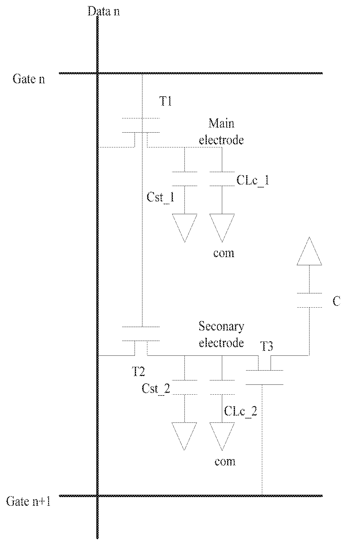
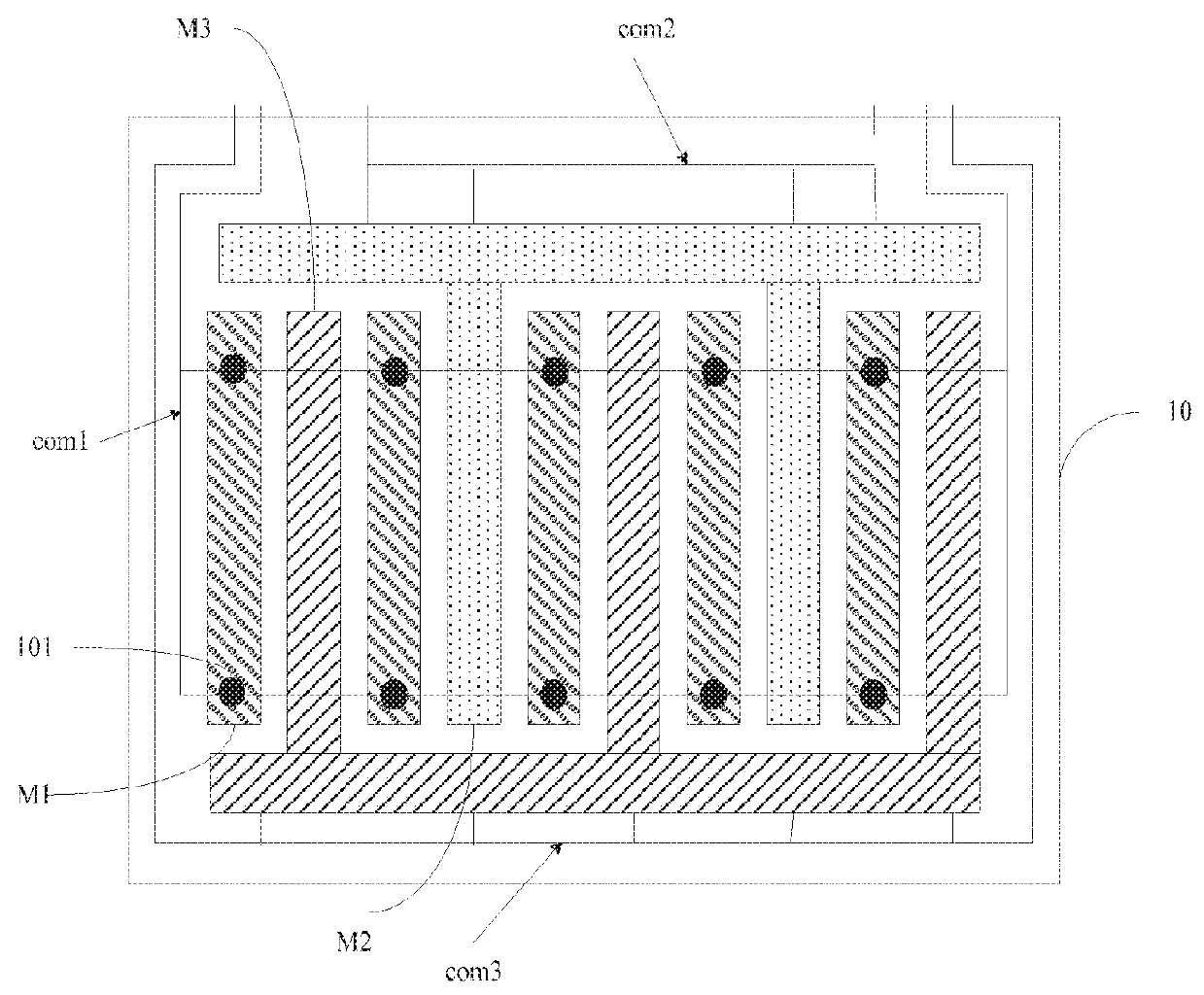
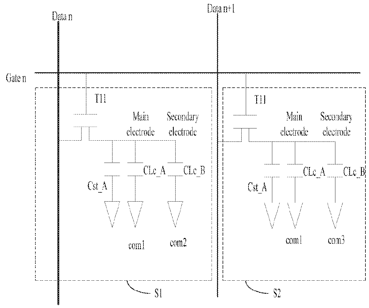
[0041]According to the present disclosure, a pixel structure comprises a common electrode, a plurality of pixel units formed by a plurality of scanning lines crossing a plurality of data lines. The common electrode comprises a first common electrode and a second common electrode set. The plurality of pixel units are formed by a plurality of scanning lines crossing a plurality of data lines. Each of the plurality of pixel units corresponds to one of the plurality of scanning lines and one of the plurality of data lines. Each of the plurality of pixel units comprises a main electrode, a secondary electrode, and a thin-film transistor (TFT). A gate of the TFT is connected to a scanning ...


PUM


Abstract

A pixel structure and a liquid crystal display panel are provided. The pixel structure includes a first common electrode, a second common electrode set, a plurality of pixel units formed by a plurality of scanning lines crossing a plurality of data lines. Each of the pixel units corresponding to one of the scanning lines and one of the data lines. Each of the pixel units includes a main electrode, a secondary electrode, and a thin-film transistor. The main electrode corresponds to the first common electrode. The secondary electrode corresponds to the second common electrode set.

Description

BACKGROUND1. Field of the Disclosure[0001]The present disclosure relates to the field of a liquid crystal display (LCD) panel, and more particularly, to a pixel structure and an LCD panel.2. Description of the Related Art[0002]A conventional vertical alignment (VA) LCD panel features a wide viewing angle, a high contrast ratio so the VA LCD panel has become a mainstream product. However, the VA LCD panel has a shortcoming of color shift. Please refer to FIG. 1 illustrating a schematic diagram of an equivalent circuit of a pixel unit of an LCD panel adopting the charge-sharing technique. The pixel electrode on each of the pixel units is divided into a main electrode and a secondary electrode. The main electrode is driven by a thin-film transistor (TFT) T1, and the secondary electrode is driven by a TFT T2, a TFT T3, and a sharing capacitor C. Specifically, the LCD panel is driven by scanning row by row. When an nth row is scanned, a scanning signal on a scanning line Gate n is at hig...

Claims


Application Information

Patent Timeline
IPC IPC(8): G02F1/1343H01L27/12G02F1/1362H01L27/32H01L33/38
CPCG02F1/1343H01L27/124H01L33/387H01L27/3248G02F1/136213G02F1/134309G09G3/3655G09G3/3659G09G2300/0426G09G2300/0465G09G2300/0876G09G2320/0242G02F1/134345H10K59/123G09G3/36
Inventor ZHANG, MENGMENGYUE, SHOUZHEN
Owner TCL CHINA STAR OPTOELECTRONICS TECH CO LTD
Why Eureka
Try Eureka