Liquid crystal displays and the pixel circuit structure thereof

a technology of liquid crystal display and pixel circuit, which is applied in the field of liquid crystal display and the pixel circuit structure thereof, can solve the problems of key issue of transmission rate and the reduction of the transmission rate of products, and achieve the effect of improving the aperture rate and the transmission ra

Active Publication Date: 2018-08-23
TCL CHINA STAR OPTOELECTRONICS TECH CO LTD
View PDF2 Cites 3 Cited by
  • Summary
  • Abstract
  • Description
  • Claims
  • Application Information

AI Technical Summary

Benefits of technology

[0003]The present disclosure relates to a LCD and the pixel circuit structure thereof, which solves the issue of low transmission rate caused by the low aperture rate of the conventional LCD.
[0006]In view of the above, with respect to the proposed pixel circuit structure, the wide viewing angle effect is not affected and the location of the first discharging capacitor is enhanced, i.e., the first discharging capacitor is arranged on the Gate. Thus, the first discharging capacitor has not occupied the aperture area, which greatly enhances the aperture rate and the transmission rate. In addition, by configuring the second discharging capacitor between the drains of the main pixel electrode and the allocation electrode, the potential of the Main PE and the Sub PE are maintained to be different, such that the LCD operate normally.

Problems solved by technology

Thus, the transmission rate is a key issue when designing the high resolution and high PPI pixels.
However, such design may sacrifice the aperture rate of the pixels, and thus the transmission rate of the products may be decreased.

Method used


Image

  • Liquid crystal displays and the pixel circuit structure thereof
  • Liquid crystal displays and the pixel circuit structure thereof
  • Liquid crystal displays and the pixel circuit structure thereof

Examples


first embodiment

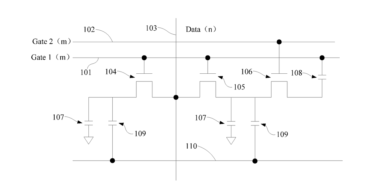
[0014]FIG. 1 is a circuit diagram of the pixel circuit structure having a high transmission rate in accordance with a first embodiment. FIG. 2 is a layout diagram of the pixel circuit structure in accordance with the first embodiment. The pixel circuit structure includes at least one first scanning line 101, at least one second scanning line 102, and at least one data line 103.

[0015]Specifically, the first scanning line 101 respectively connects to gates of a main pixel electrode 104 and a second pixel electrode 105. The first scanning line 101 controls the main pixel electrode 104 (Main) and the second pixel electrode 105 (Sub TFT). The second scanning line 102 connects to a gate of an allocation electrode 106, and controls the transistor of the allocation electrode 106 (Sharing TFT) to discharge to a pixel electrode (Sub PE).

[0016]The sources of the main pixel electrode 104 and the second pixel electrode 105 respectively connects to a data line 103, and the drains of the main pixe...

second embodiment

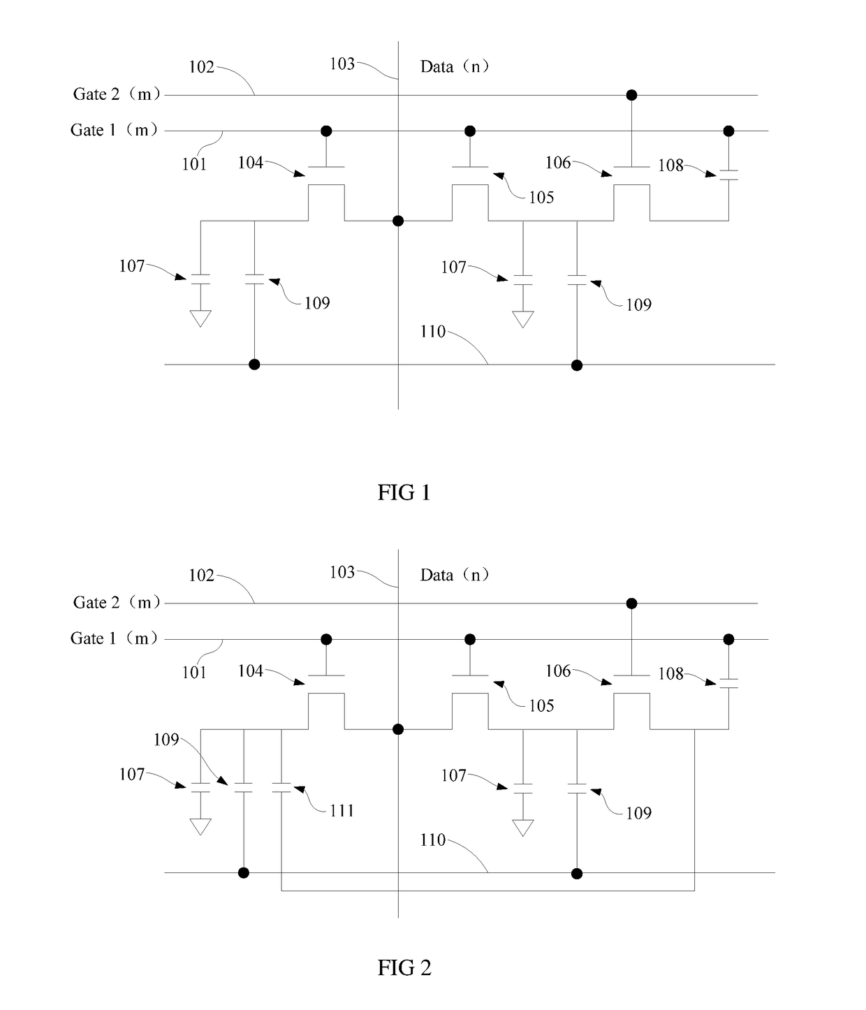
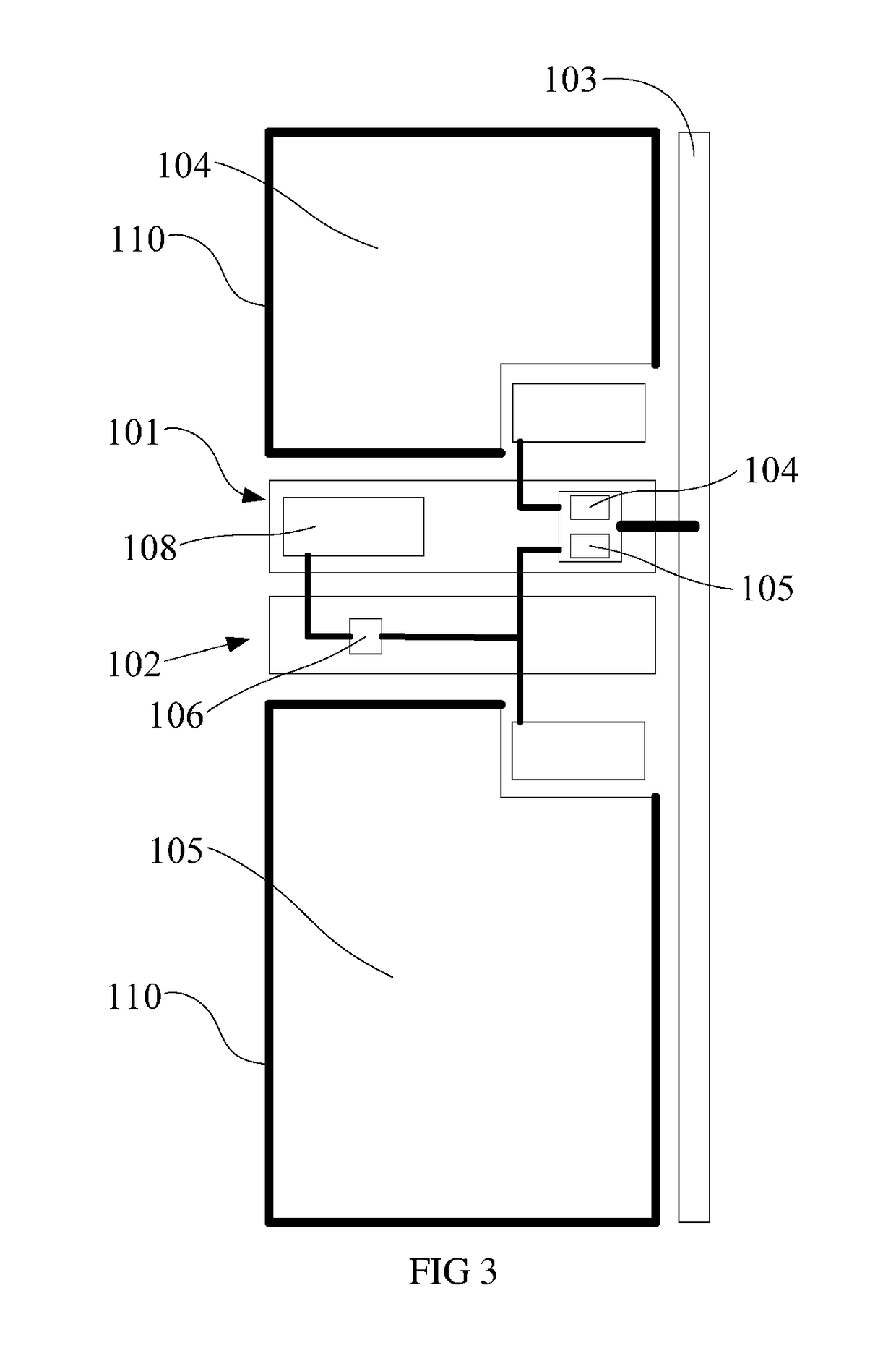
[0023]FIG. 3 is a circuit diagram of the pixel circuit structure having a high transmission rate in accordance with the second embodiment. FIG. 4 is a layout diagram of the pixel circuit structure in accordance with the second embodiment. The pixel circuit structure includes at least one first scanning line 101, at least one second scanning line 102, and at least one data line 103.

[0024]Specifically, the first scanning line 101 respectively connects to the gates of a main pixel electrode 104 and a second pixel electrode 105. The first scanning line 101 controls the main pixel electrode 104 (Main) and the second pixel electrode 105 (Sub TFT). The second scanning line 102 connects to a gate of an allocation electrode 106, and controls the transistor of the allocation electrode 106 (Sharing TFT) to discharge to a pixel electrode (Sub PE).

[0025]The sources of the main pixel electrode 104 and the second pixel electrode 105 respectively connects to a data line 103, and the drains of the m...


PUM

PropertyMeasurementUnit
voltagesaaaaaaaaaa
voltagesaaaaaaaaaa
blinking timeaaaaaaaaaa

Abstract

The present disclosure relates to a liquid crystal panel and the pixel circuit structure thereof. The pixel circuit structure includes at least one first scanning line, at least one second scanning line, and at least one data line. A source of the allocation electrode connects to the drain of the second pixel electrode, and a first discharging capacitor is arranged between the source and the first scanning line. With respect to the proposed pixel circuit structure, the wide viewing angle effect is not affected and the location of the first discharging capacitor is enhanced, i.e., the first discharging capacitor is arranged on the Gate. Thus, the first discharging capacitor has not occupied the aperture area, which greatly enhances the aperture rate and the transmission rate.

Description

BACKGROUND OF THE INVENTION1. Field of the Invention[0001]The present disclosure relates to liquid crystal display technology, and more particularly to a liquid crystal display (LCD) and the pixel circuit structure thereof.2. Discussion of the Related Art[0002]The performance of the high resolution and high pixel per inch (PPI) is precise and fine so as to provide a high resolution display, which has been a main trend of display technology. The dimension of the pixels is also decreased when the resolution and the PPI are increased. With the decrease of the dimensional of the pixels, a ratio of a metal dimension to the unit dimension is increased, which resulting in that the corresponding aperture rate is decreased, and the corresponding transmission rate is decreased. Thus, the transmission rate is a key issue when designing the high resolution and high PPI pixels. Generally, vertical alignment (VA) mode has been designed with wide viewing angle compensation. i.e., which includes a ...

Claims


Application Information

Patent Timeline
Patent Type & Authority Applications(United States)
IPC IPC(8): G02F1/1362G02F1/1368H01L27/12
CPCG02F1/136286G02F1/1368H01L27/124G02F2201/121G02F2201/123G02F1/136213G09G3/364G09G3/3659G09G2300/0426G09G2300/0447G09G2300/0465
Inventor YING, JIANJIAN
Owner TCL CHINA STAR OPTOELECTRONICS TECH CO LTD
Why Eureka
Try Eureka