Black electrode, method of manufacturing black electrode substrate and display device

a technology of black electrode and substrate, which is applied in the direction of conductive layers on insulating supports, instruments, conductors, etc., can solve the problems of difficult to achieve the input of pen input onto the touch panel, difficult to avoid an increase of the thickness of the display device, and the touch panel is considered an unnecessary componen

Active Publication Date: 2017-04-27
TOPPAN PRINTING CO LTD
View PDF2 Cites 23 Cited by
  • Summary
  • Abstract
  • Description
  • Claims
  • Application Information

AI Technical Summary

Benefits of technology

[0068]Even when indium is used as a metal, or indium is used as an oxide, adhesion strength of the indium-containing layer can be significantly improved with respect to a resin such as acrylic resin which is a base material of a color filer, a transparent substrate such as of glass, or an inorganic film made of silicon oxide, silicon nitride or the like. Therefore, an indium-containing layer can be provide at a boundary surface between a metal layer (i.e., copper-containing layer) formed of copper or copper alloy and a black layer, or at a boundary surface between the transparent substrate or an inorganic insulation layer and the metal layer. Even when indium is used as a metal, or indium is used as an oxide, by providing the indium-containing layer at the terminal portion, a terminal portion having good electrical connectivity can be provided.

Problems solved by technology

Accordingly, the touch panel is considered as an unnecessary component in this structure of the display device.
However, even with this type of touch panel, it is difficult to avoid an increase of the entire thickness of the display device.
Further, in the case where the display device is provided with the above-mentioned touch panel and high definition pixels, there is a disadvantage that necessary input (pen input) onto the touch panel is difficult to achieve.
Thus, if the display device has the above-mentioned touch panel and such high definition pixels, most of touch panels do not tolerate the pen pressure of the pen.
Moreover, such display devices raise problems, including a problem of limited resolution in the opening configuring the input portion of the touch panel, or a problem of difficulty in achieving sufficient resolution of the touch panel to obtain high definition of the display device.
Therefore, the organic film base material is difficult to use for high-definition color filter substrates.

Method used


Image

  • Black electrode, method of manufacturing black electrode substrate and display device
  • Black electrode, method of manufacturing black electrode substrate and display device
  • Black electrode, method of manufacturing black electrode substrate and display device

Examples


first embodiment

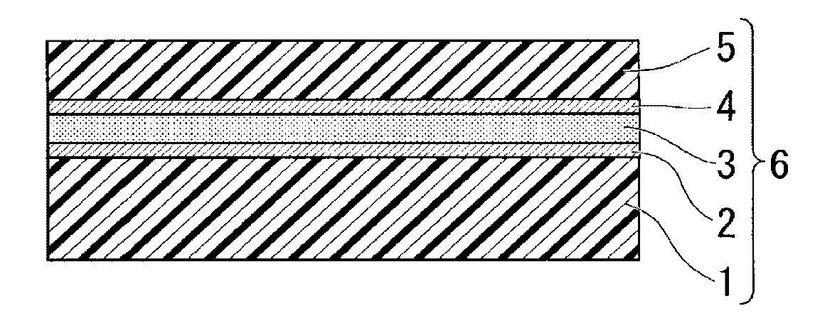
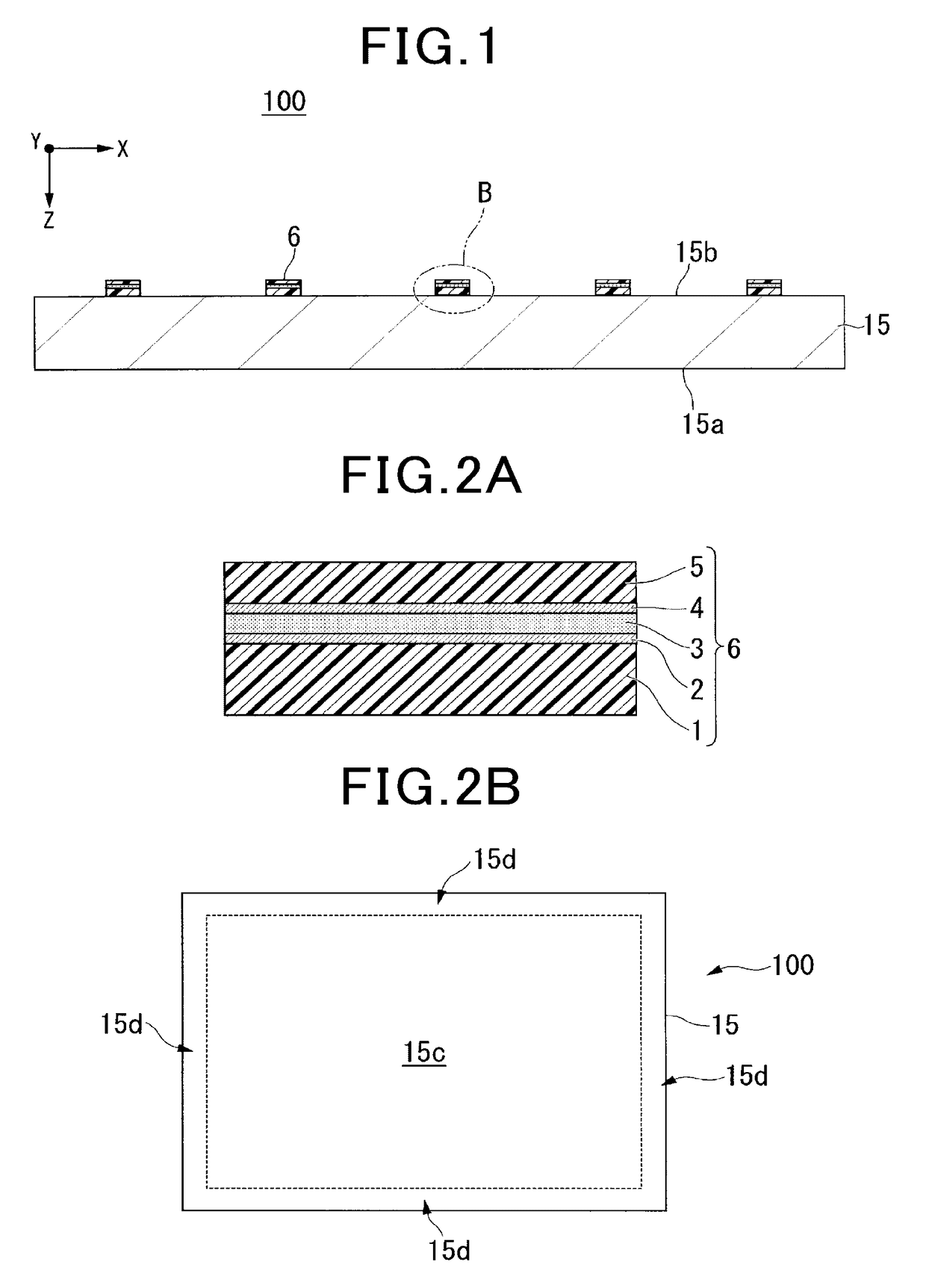
[0043]Hereinafter, with reference to FIGS. 1 to 3, a black electrode substrate 100 according to an embodiment of the present invention will be described.

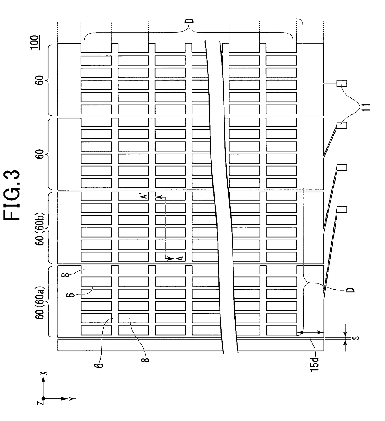
[0044]FIG. 1 illustrates a minimum configuration of a black electrode substrate according to the present embodiment. The black electrode substrate 100 is provided with a transparent substrate 15, and a plurality of black wirings 6 provided on the transparent substrate 15. The cross-sectional view of FIG. 1 illustrates that the plurality of black wirings 6 are disposed on the transparent substrate 15. As shown in plan view of FIG. 3, the black wiring 6 configures a black electrode pattern 60 having a plurality of pixel opening portions 8. In other words, regions formed between the plurality of black wirings 6 shown in FIG. 1 correspond to the pixel opening portion 8. A display portion, a shape of the opening, the number of pixels of the display device, which will be described later in detail, are not limited to the above-mentioned co...

second embodiment

[0078]FIG. 4 is a cross-sectional view showing a part of black electrode substrate according to the second embodiment, and showing a structure in which a red layer, a green layer and a blue layer are provided on the pixel opening portions.

[0079]In the pixel opening portion 8, a color filter can be laminated to partially overlap an end portion of the second black layer 5. The color filter is composed of colored layers such as a red layer R, a green layer G, and a blue layer B. Further, a transparent resin layer 9 is formed to cover the red layer R, the green layer G, and the blue layer B. To the color filter, other than colored layers of the red layer R, the green layer G and the blue layer B, other color layers can be added, including a light color layer, a complementary color layer, a white layer (transparent layer). Prior to laminating the color filter corresponding to the pixel opening portion 8, the transparent resin layer may be formed on the second surface 15b of the transpare...

third embodiment

[0081](Vertical Electric Field Type Liquid Crystal Display Device)

[0082]Next, with reference to FIGS. 5 to 10, a liquid crystal display device according to a third embodiment of the present invention will be described. In the third embodiment, the same reference signs are designated to the same elements as the first and second embodiments, and the description is omitted or simplified.

[0083]FIG. 5 is a block diagram for explaining functions of the liquid crystal display device according to the present embodiment. A liquid crystal display device 500 according to the present embodiment is provided with a display unit 110, a control unit 120 for controlling the display unit 110 and a touch sensing function. The control unit 120 having a publicly known configurations is provided with a video signal timing control unit 121, a touch sensing / scan signal control unit 122 and a system control unit 123.

[0084]The video signal timing control unit 121 controls a plurality of transparent conductiv...


PUM

PropertyMeasurementUnit
sizeaaaaaaaaaa
thicknessaaaaaaaaaa
reflectanceaaaaaaaaaa

Abstract

A black electrode substrate includes a transparent substrate having a first surface and a second surface opposite to the first surface, the second surface having a display region in a rectangular shape in plan view and an outer region outside of the display region, a black wiring forming a black electrode pattern that defines a plurality of pixel opening portions in the display region, and a transparent resin layer formed in the display region such that the transparent resin layer has the same rectangular shape as the display region in plan view. The black wiring has a laminated structure including a first black layer, a first indium-containing layer, a copper-containing layer, a second indium-containing layer, and a second black layer. The black wiring has a terminal portion formed such that the second indium-containing layer positioned in the outer region is exposed from the laminated structure.

Description

CROSS-REFERENCE TO RELATED APPLICATIONS[0001]The present application is a continuation of and based upon and claims the benefits of priority to International Application No. PCT / JP2014 / 068446, filed Jul. 10, 2014. The entire contents of this application are incorporated herein by reference.BACKGROUND OF THE INVENTION[0002]Field of the Invention[0003]The present invention relates to a black electrode substrate provided with a metal wiring having low resistance and improving visibility thereof, a method of manufacturing a black electrode substrate and a display apparatus provided with the black electrode substrate.[0004]The black electrode substrate is used for an in-cell type display device integrating capacitive type touch sensing functionality into the liquid crystal cell.[0005]Discussion of the Background[0006]Generally, display devices configured to use a touch panel are well known. The touch panel is disposed on a display surface of a display device which is provided in portable...

Claims


Application Information

Patent Timeline
Patent Type & Authority Applications(United States)
IPC IPC(8): G06F3/041G02F1/1368G02F1/1362G02F1/1343G06F3/044G02F1/1333
CPCG06F3/0412G06F3/044G06F3/0416G02F1/13338G02F1/136286G02F1/134363G02F2001/134372G02F1/13439G02F2203/01G06F2203/04103G02F2001/136295G02F2001/13629G02F2201/121G02F1/1368H01B5/14G06F3/0443G06F3/04166G06F3/04164G06F3/0445G06F3/0446H01B1/026G02F1/13629G02F1/134372G02F1/136295
Inventor KIMURA, YUKIHIROFUKUYOSHI, KENZO
Owner TOPPAN PRINTING CO LTD
Why Eureka
Try Eureka