Thin film transistor array substrate and liquid crystal display panel

a thin film transistor array and liquid crystal display technology, applied in semiconductor devices, semiconductor/solid-state device testing/measurement, instruments, etc., can solve the problems of unsatisfactory display results of the entire liquid crystal display panel, large rc loading of the pixel in prior art, etc., to reduce the capacitance between the common electrode layer and the sensing wire, reduce the rc loading of the pixel, and reduce the overlap

Active Publication Date: 2017-09-14
TCL CHINA STAR OPTOELECTRONICS TECH CO LTD +1
View PDF2 Cites 1 Cited by
  • Summary
  • Abstract
  • Description
  • Claims
  • Application Information

AI Technical Summary

Benefits of technology

[0021]Compared with prior art, in the thin film transistor array substrate and the liquid crystal display panel of the present invention, the first strip holes are located at the common electrode layer, and the first strip holes are located corresponding to the sensing wires to decrease the overlapping area between the common electrode layer and the sensing wires. Accordingly, the capacitance between the common electrode layer and the sensing wires is decreased to reduce the RC loading of the pixel and to promote the display quality of the liquid crystal display panel utilizing the thin film transistor array substrate.

Problems solved by technology

In conclusion, the RC loading of the pixel in prior art is larger, and the display result of the entire liquid crystal display panel is not ideal.

Method used


Image

  • Thin film transistor array substrate and liquid crystal display panel
  • Thin film transistor array substrate and liquid crystal display panel
  • Thin film transistor array substrate and liquid crystal display panel

Examples


Embodiment Construction

[0029]Embodiments of the present invention are described in detail with the technical matters, structural features, achieved objects, and effects with reference to the accompanying drawings as follows. It is clear that the described embodiments are part of embodiments of the present invention, but not all embodiments. Based on the embodiments of the present invention, all other embodiments to those of ordinary skill in the premise of no creative efforts obtained, should be considered within the scope of protection of the present invention.

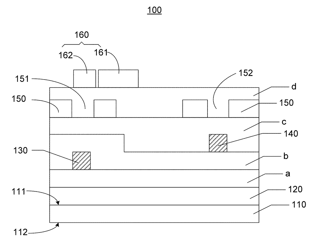
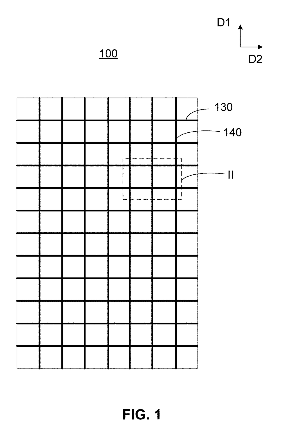
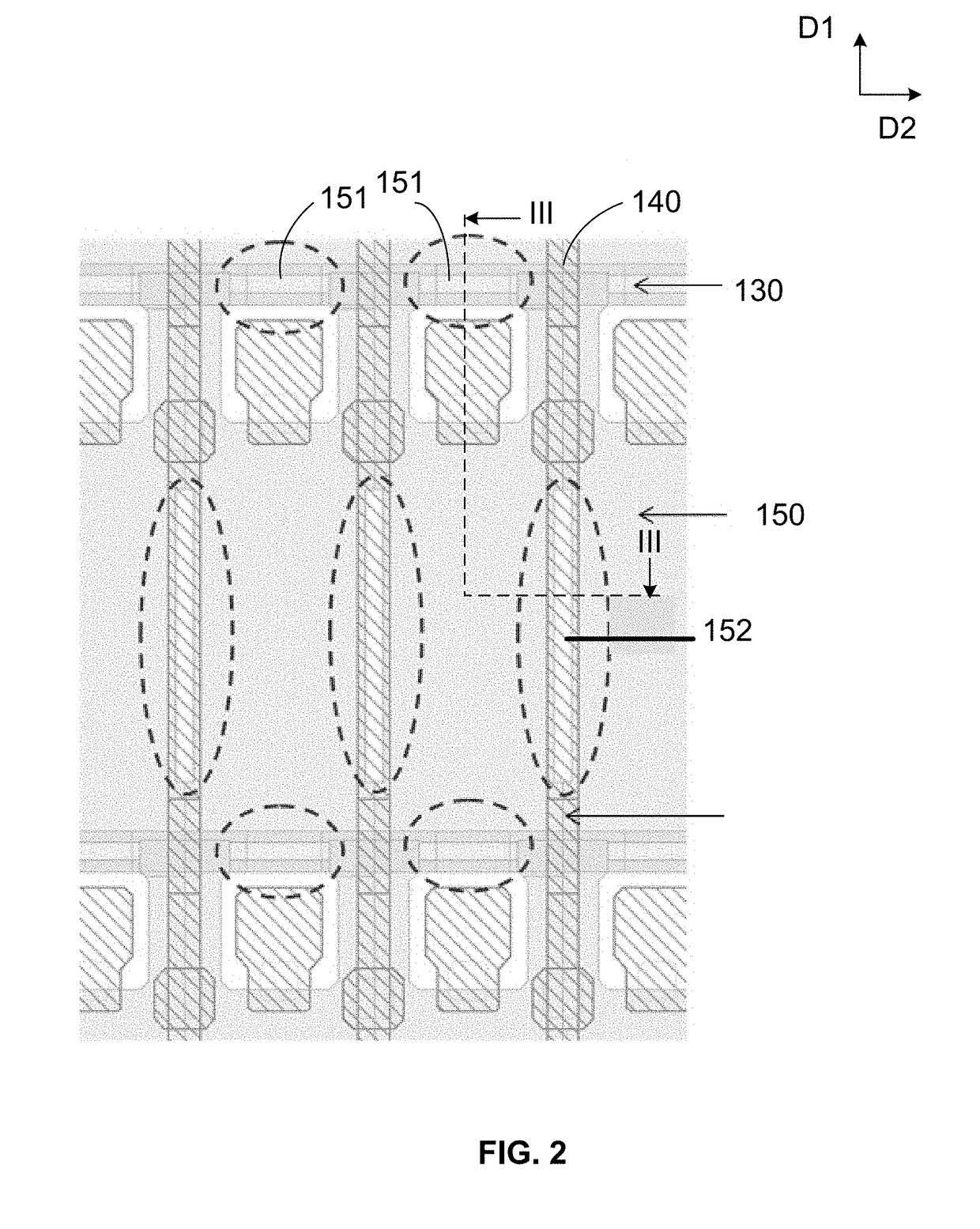
[0030]Please refer to FIG. 1, FIG. 2 and FIG. 3. FIG. 1 is a structure diagram of a thin film transistor array substrate according to on preferred embodiment of the present invention; FIG. 2 is an enlarged structure diagram of II position in FIG. 1 of the present invention; FIG. 3 is a sectional structure diagram of III-III in FIG. 2 of the present invention. The thin film transistor array substrate 100 comprises a substrate 110, a thin film transi...


PUM

PropertyMeasurementUnit
widthaaaaaaaaaa
volumeaaaaaaaaaa
weightaaaaaaaaaa

Abstract

The present invention provides a thin film transistor array substrate and a liquid crystal display panel. The thin film transistor array substrate comprises: a substrate, and the substrate comprises a first surface and a second surface oppositely located; a thin film transistor array, located on the first surface; a common electrode layer, and the common electrode layer is isolated from the thin film transistor array, and the common electrode layer comprises a plurality of first strip holes; a sensing electrode layer, and the sensing electrode layer is isolated from the common electrode layer, and the sensing electrode layer comprises a plurality of sensing units and a plurality of sensing wires, and the sensing units are distributed in row and column, and the sensing wires are electrically coupled to the sensing units of each row or each column respectively, and the sensing wires are located corresponding to the first strip holes.

Description

CROSS REFERENCE[0001]This application claims the priority of Chinese Patent Application No. 201510626558.5, entitled “Thin film transistor array substrate and liquid crystal display panel”, filed on Sep. 28, 2015, the disclosure of which is incorporated herein by reference in its entirety.FIELD OF THE INVENTION[0002]The present invention relates to a display skill field, and more particularly to a Thin film transistor array substrate and a liquid crystal display panel.BACKGROUND OF THE INVENTION[0003]The liquid crystal display (LCD) is a common electronic apparatus. It is favored by the users with its properties of low power consumption, small volume and light weight. The touch and display merge is also the popular field of the display panel researches, and the Low Temperature Poly-Silicon (LTPS) is considered to be the high end technology of the field. The in cell technology is to embed the touch panel function into the liquid crystal pixel. In the design process of the traditional...

Claims


Application Information

Patent Timeline
Patent Type & Authority Applications(United States)
IPC IPC(8): G02F1/1362G06F3/041G02F1/1333G02F1/1368
CPCG02F1/136286G02F1/1368G06F3/041H01L27/124G02F2201/121G02F2001/13606G02F1/13338H01L22/32G06F3/0412G02F1/1333G06F3/0445G06F3/0446G02F1/13606
Inventor CHEN, GUICHEN, CAIQIN
Owner TCL CHINA STAR OPTOELECTRONICS TECH CO LTD
Why Eureka
Try Eureka