Array substrate and touch display device

Active Publication Date: 2018-05-10
WUHAN CHINA STAR OPTOELECTRONICS TECH CO LTD
View PDF0 Cites 5 Cited by
  • Summary
  • Abstract
  • Description
  • Claims
  • Application Information

AI Technical Summary

Benefits of technology

[0017]The present disclosure achieves the following beneficial effects. According to the present disclosure, the display scan and the touch scan can be performed in time-sharing manner. When an image is displayed, the drive scan line transmits the scan signal, which enables the first common electrode and the second common electrode to be connected through the common transistor and have a same electric potential, thus supplying a common voltage for display of each of the pixel units. When a touch scan is performed, the touch scan line transmits the scan signal, which enables the touch transistor to conduct. In this manner, each of the second common electrodes will be able to independently transm

Problems solved by technology

Therefore, in the process of manufacturing the array substrate, it is required to add at least one pho

Method used


Image

  • Array substrate and touch display device
  • Array substrate and touch display device
  • Array substrate and touch display device

Examples


Example

[0027]The present disclosure will be explained in detail below with reference to the embodiments and the accompanying drawings, so that one can fully understand how the present disclosure solves the technical problem and achieves the technical effects through the technical means, thereby implementing the same. It should be noted that as long as there is no structural conflict, any of the embodiments and any of the technical features thereof may be combined with one another, and the technical solutions obtained therefrom all fall within the scope of the present disclosure.

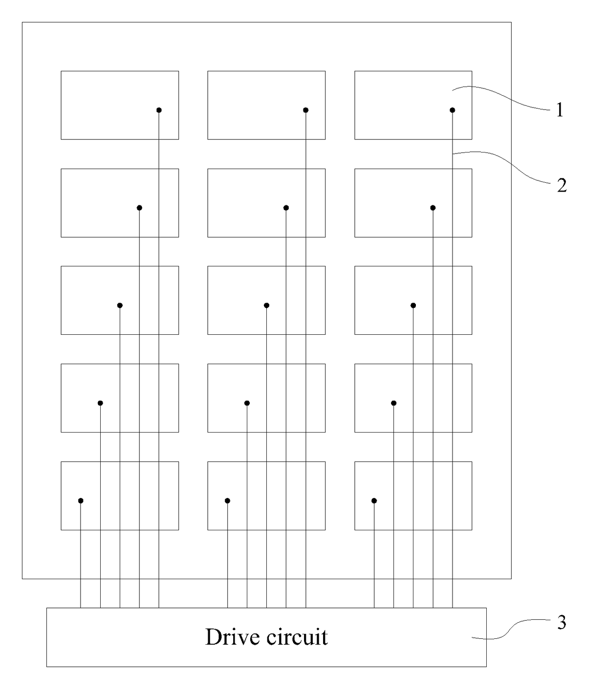
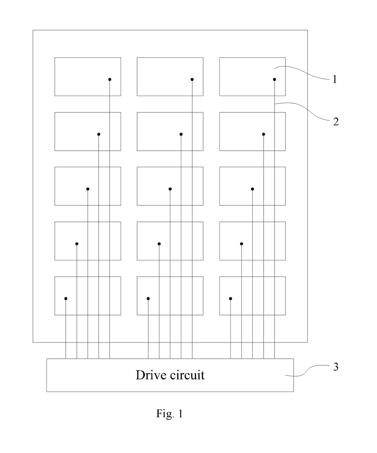
[0028]The present embodiment provides a touch display device which can be used in electronic products such as mobile phones, tablet PCs, etc. The touch display device comprises an array substrate, a drive circuit, etc.

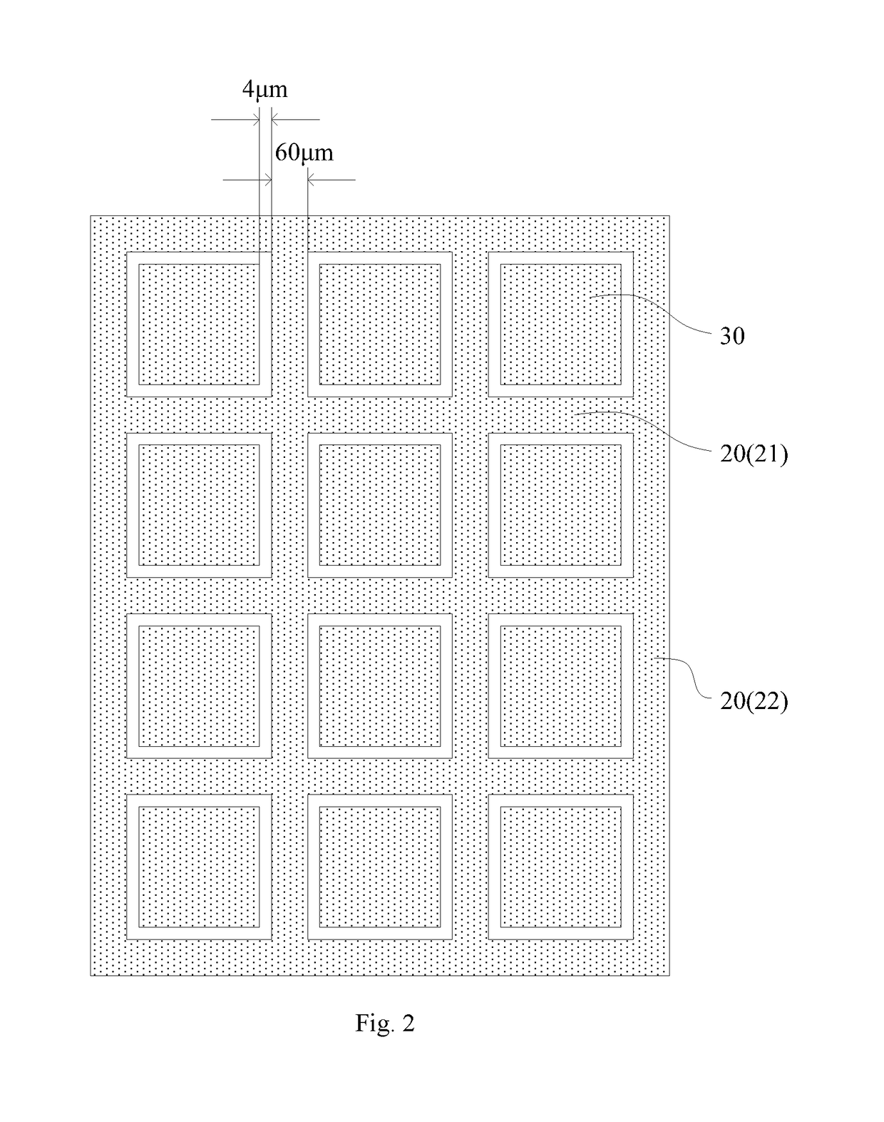
[0029]As shown in FIGS. 2 and 3, the array substrate comprises a pixel unit array formed by a drive scan line PG and a data line D. Each of the pixel units is provided therein with a drive transistor T...


PUM


Abstract

Disclosed is an array substrate and touch display device which belongs to the technical filed of display and is able to solve the technical problem that in the existing technologies, the process of manufacturing an array substrate is too complex. The array substrate includes a drive scan line, a data line, a first common electrode, a second common electrode, a touch scan line, a common transistor, and a touch transistor. The first common electrode and the second common electrode are arranged in a spaced-apart manner. A source and a drain of the common transistor are connected respectively to the first common electrode and the second common electrode, and a gate of the common transistor is connected to the drive scan line. A source and a drain of the touch transistor are connected respectively to the data line and the second common electrode, and a gate of the touch transistor is connected to the touch scan line.

Description

CROSS-REFERENCE TO RELATED APPLICATIONS[0001]The present application claims the priority of Chinese patent application CN201510566336.9, entitled “Array substrate and touch display device” and filed on Sep. 7, 2015, the entirety of which is incorporated herein by reference.TECHNICAL FIELD[0002]The present disclosure relates to the technical field of display, and in particular, to an array substrate and a touch display device.TECHNICAL BACKGROUND[0003]With the development of display technology, liquid crystal display devices have become the most common display devices.[0004]In the meanwhile, with the popularization of smart electronic products, capacitive touch screens are also widely used in electronic products, such as cell phones, tablet PCs, etc. Currently, capacitive touch screens mainly adopt one glass solution (OGS), on-cell, and in-cell technologies. Compared with OGS and on-cell technologies, in-cell technology is superior in production process, and products using it are thi...

Claims


Application Information

Patent Timeline
IPC IPC(8): G02F1/1333G02F1/1343G06F3/041G02F1/1362
CPCG02F1/13338G02F1/1343G06F3/0412G02F1/136286G09G2310/0264G02F1/134309G02F1/1368G02F2201/121G06F3/04164G06F3/04166G06F3/0443G02F1/134318G02F1/1333G02F1/1362
Inventor TSAI, YUCHENGHUANG, YAO LICAO, CHANG
Owner WUHAN CHINA STAR OPTOELECTRONICS TECH CO LTD
Why Eureka
Try Eureka