Liquid crystal display device and method of manufacturing the same

Active Publication Date: 2006-05-11
LG DISPLAY CO LTD
View PDF20 Cites 16 Cited by
  • Summary
  • Abstract
  • Description
  • Claims
  • Application Information

AI Technical Summary

Benefits of technology

[0029] An object of the present invention is to provide a liquid crystal display device and a method of manufacturing the same in which manufacturing processes are simplified

Problems solved by technology

Accordingly, when light or an electric field is applied thereto, amorphous silicon is changed into a quasi-stable state, which is unstable for use as a TFT.
More specifically, the electrical characteristics of the amorphous silicon degrade as a result of light irradiation, and thus light irradiated a-Si is difficult to use for a driving circuit due to its low electric field mobility (0.1-1.0 cm2/V·s) and low reliability.
Also, since the a-Si TFT array substrate and a printed circuit board (PCB) with the driving IC for the a

Method used


Image

  • Liquid crystal display device and method of manufacturing the same
  • Liquid crystal display device and method of manufacturing the same
  • Liquid crystal display device and method of manufacturing the same

Examples


Embodiment Construction

[0045] Reference will now be made in detail to the preferred embodiments of the present invention, examples of which are illustrated in the accompanying drawings. Wherever possible, the same reference numbers will be used throughout the drawings to refer to the same or like parts.

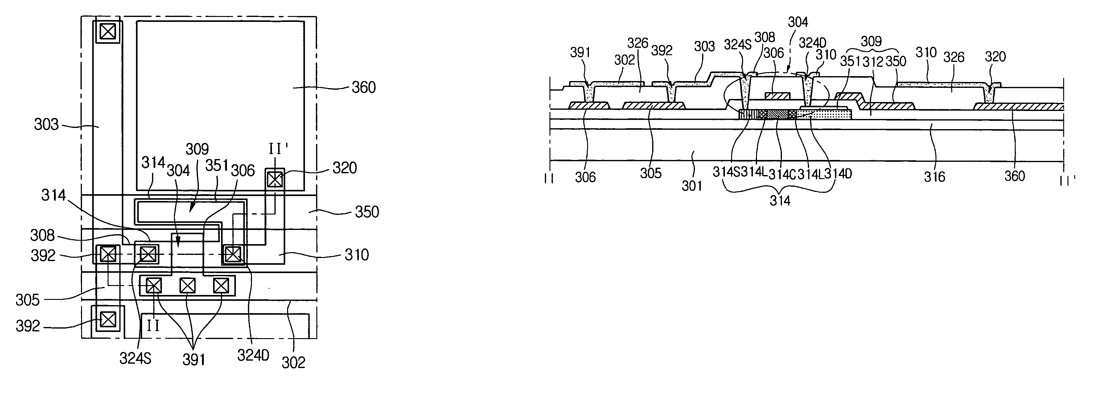
[0046]FIG. 3 is a plan view of an array substrate of an LCD according to an embodiment of the present invention, and FIG. 4 is a cross-sectional view taken along line I-I′ in FIG. 3.

[0047] Referring to FIGS. 3 and 4, a gate line 202 and a data line segment 203 are arranged perpendicularly with respect to each other and are insulated from each other. A TFT 204 is disposed adjacent to where the gate line 202 and the data line segment 203 are closest to each other. A pixel region is defined between the gate line 202 and the data line segment 203. A pixel electrode 260 is connected to the TFT 204 and disposed within the pixel region. A gate electrode 206 of transparent conductive material is connected from th...


PUM


Abstract

A liquid crystal display device including first and second active layers over a substrate, a storage line over the second active layer, a first insulating layer over the storage line, a gate electrode on the first insulating layer and corresponding to the first active layer, a second insulating layer over the gate electrode, source and drain electrodes connected to the first active layer through the first and second insulating layers, a gate line connected to the gate electrode through the second insulating layer, a data line substantially perpendicularly arrange with respect to the gate line to define a pixel region, a pixel electrode connected to the drain electrode through the second insulating layer, and a connection line connected to one of the gate line and the data line through the second insulating layer.

Description

[0001] The present invention claims the benefit of Korean Patent Application No. 090334 / 2004 filed in Korea on Nov. 8, 2004, which is hereby incorporated by reference in its entirety. BACKGROUND OF THE INVENTION [0002] 1. Field of the Invention [0003] The present invention relates to a liquid crystal display (LCD), and more particularly, to an array substrate of an LCD and a method of manufacturing the same. [0004] 2. Description of the Related Art [0005] An LCD is considered to be the next generation of display device because it has good portability and low power consumption, and also has a good performance in terms of resolution and digital adaptability. The LCD is a non-self-luminous display device in which liquid crystal is positioned between a color filter substrate and an array substrate having a thin film transistor (TFT). An image is displayed by using the anisotropy of the liquid crystal and the different refractivity of light transmitted through the LCD from a backlight un...

Claims


Application Information

Patent Timeline
IPC IPC(8): H01L29/76
CPCG02F1/13454G02F1/136213H01L27/1288H01L29/78621H01L27/1255G02F2001/136236G02F1/136236G02F1/136
Inventor YANG, JOON YOUNG
Owner LG DISPLAY CO LTD
Why Eureka
Try Eureka