Display Device with Touch Sensor

Active Publication Date: 2018-04-05
LG DISPLAY CO LTD
View PDF4 Cites 16 Cited by
  • Summary
  • Abstract
  • Description
  • Claims
  • Application Information

AI Technical Summary

Benefits of technology

[0008]In one embodiment, an organic light emitting display device with a touch sensor removes the necessity of an additional adhesion process by directly disposing a touch sensing electrode and a tou

Problems solved by technology

In this case, there are problems of complicated overall process and increased costs resulting from an additional attach

Method used


Image

  • Display Device with Touch Sensor
  • Display Device with Touch Sensor
  • Display Device with Touch Sensor

Examples


first embodiment

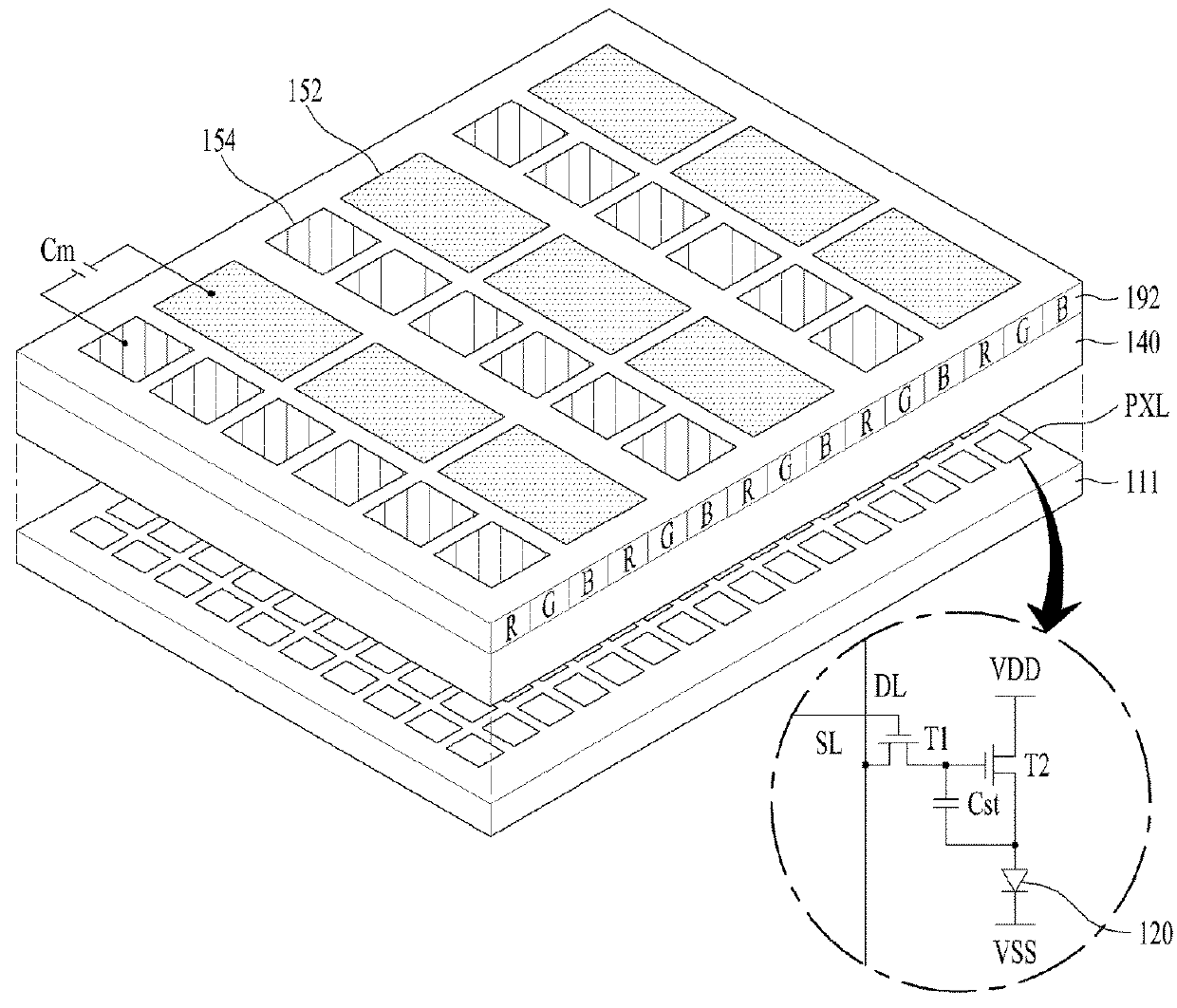
[0054]As such, the organic light emitting display device with a touch sensor according to the present disclosure has a structure in which the touch sensing electrode 152 and the touch driving electrode 154 are formed on the encapsulation layer 140 during manufacturing of the display. Accordingly, as compared to a related organic light emitting display device in which a touchscreen is directly attached to the organic light emitting display device by an adhesive agent, the present disclosure does not require an adhesion process, thus simplifying the manufacturing process and reducing manufacturing costs.

[0055]All the layers shown in FIG. 3 as formed on a single substrate 111. In one embodiment, substrate 111 may be the only substrate in the display device.

second embodiment

[0056]FIG. 4 is a sectional view illustrating an organic light emitting display device with a touch sensor according to the present disclosure.

[0057]The organic light emitting display device with a touch sensor illustrated in FIG. 4 includes the same elements as the organic light emitting display device illustrated in FIG. 3, except that the touch driving electrode 154 and the touch sensing electrode 152 are disposed on a touch buffer layer 166. The touch driving electrode 154 and the touch sensing electrode 152 are in a same plane. Accordingly, detailed description of the same elements will be omitted.

[0058]The touch buffer layer 166 is formed on the color filter 192 and the black matrix 194 so as to cover the color filter 192 and the black matrix 194. The touch sensing electrode 152, the touch driving electrode 154 and the routing line 180 are formed on the touch buffer layer 166. The location of the touch buffer layer 166 causes it to be between the touch electrodes 152 and 154 a...

third embodiment

[0065]FIG. 5 is a sectional view illustrating an organic light emitting display device with a touch sensor according to the present disclosure.

[0066]The organic light emitting display device illustrated in FIG. 5 includes the same elements as the organic light emitting display device illustrated in FIG. 4, except that the touch driving electrode 154 and the touch sensing electrode 152 are disposed in parallel on the second inorganic encapsulation layer 146, which is the uppermost layer of the encapsulation layer 140. Accordingly, detailed description of the same elements will be omitted.

[0067]The color filter 192 and the black matrix 194 illustrated in FIG. 5 cover the touch sensor. That is, the touch driving electrode 154 and the touch sensing electrode 152 included in the touch sensor are disposed between the color filter 192 and the encapsulation layer 140. In this case, the color filter 192 and the black matrix 194, which are disposed higher than the touch sensor, absorb exterio...


PUM


Abstract

Disclosed are an organic light emitting display device and a method of manufacturing the same to reduce thickness and weight. The organic light emitting display device with a touch sensor removes the necessity of an additional adhesion process by directly forming a touch sensing electrode and a touch driving electrode arranged in parallel and a color filter on an encapsulation layer covering a light emitting device, thereby simplifying a manufacturing process and reducing manufacturing costs.

Description

CROSS REFERENCE TO RELATED APPLICATIONS[0001]This application claims the benefit of Korean Patent Application No. 10-2016-0126760, filed on Sep. 30, 2016, which is hereby incorporated by reference as if fully set forth herein.BACKGROUNDField[0002]An embodiment of the present disclosure relates to an organic light emitting display device with a touch sensor and a method of manufacturing the same, and more particularly, to an organic light emitting display device with a touch sensor and a method of manufacturing the same to simplify a manufacturing process and reduce manufacturing costs.Discussion of the Related Art[0003]A touchscreen is a device for inputting a user's command by selecting an instruction shown on a screen of a display or the like with the hand of the user or an object. That is, the touchscreen converts a contact position thereof that directly contacts the hand of the user or the object into an electrical signal and receives the instruction selected in the contact posi...

Claims


Application Information

Patent Timeline
IPC IPC(8): G06F3/041G06F3/0354G06F3/044F21V9/08H01L51/52H01L27/32
CPCG06F3/0412G06F3/03547G06F3/044F21V9/08H01L51/5253H01L27/323H01L2227/323H01L51/5284H01L27/3244G06F2203/04103G06F2203/04112F21Y2115/15H01L27/322H10K59/40G06F3/04164G06F3/0443H10K59/38H10K59/131H10K50/841H10K59/1201H10K50/13H10K50/844H10K71/00G06F3/0446H10K50/865H10K59/12
Inventor LEE, JAE-WONNAM, SEUNG-HEEKIM, MIN-JOOPARK, KWON-SHIKOH, JAE-YOUNGLEE, DEUK-SULEE, BU-YEOLLEE, EUN-HYE
Owner LG DISPLAY CO LTD
Why Eureka
Try Eureka