Semiconductor device and method of manufacturing the same

Inactive Publication Date: 2010-10-14
RENESAS ELECTRONICS CORP
View PDF4 Cites 14 Cited by
  • Summary
  • Abstract
  • Description
  • Claims
  • Application Information

AI Technical Summary

Benefits of technology

[0020]An exemplary aspect of the present invention is a semiconductor device having a vertical MOSFET that includes a first trench that is formed in a semiconductor substrate and includes a gate electrode of the vertical MOSFET embedded therein with a gate insulating film interposed therebetween, a second trench that is connected with the first trench and has a trench width wider than the first trench, a gate pad that is connected with the gate electrode and formed to a sidewall of the second trench with the gate insulating film interposed therebetween, and a gate line that is connected with a sidewall of the gate pad and electrically connects with the gate electrode via the gate pad. This achieves the configuration in which the gate pads formed respectively to opposing sidewalls in the second trench are apart from each other, which are provided to obtain a contact with the gate electrode and the gate line. This enables to reduce the cost and simplify the wafer manufacturing process.
[0021]Another exemplary aspect of the present invention is a method of manufacturing a semiconductor device having a vertical MOSFET th

Problems solved by technology

This is a limitation in the outer peripheral design.
Therefore, there is a problem that the number of wafer manufacturing process increases.
Therefore, the present inventor has found a problem that there is a problem of l

Method used


Image

  • Semiconductor device and method of manufacturing the same
  • Semiconductor device and method of manufacturing the same
  • Semiconductor device and method of manufacturing the same

Examples


Example

[0031]Hereinafter, an exemplary embodiment of the present invention is described with reference to the drawings. For clarity of explanation, the following descriptions and drawings are omitted and simplified as appropriate. Moreover, for clarity of explanation, repeated explanation is omitted as necessary. Note that the same components in the drawings are denoted by the same reference numerals and the explanation thereof is omitted as appropriate.

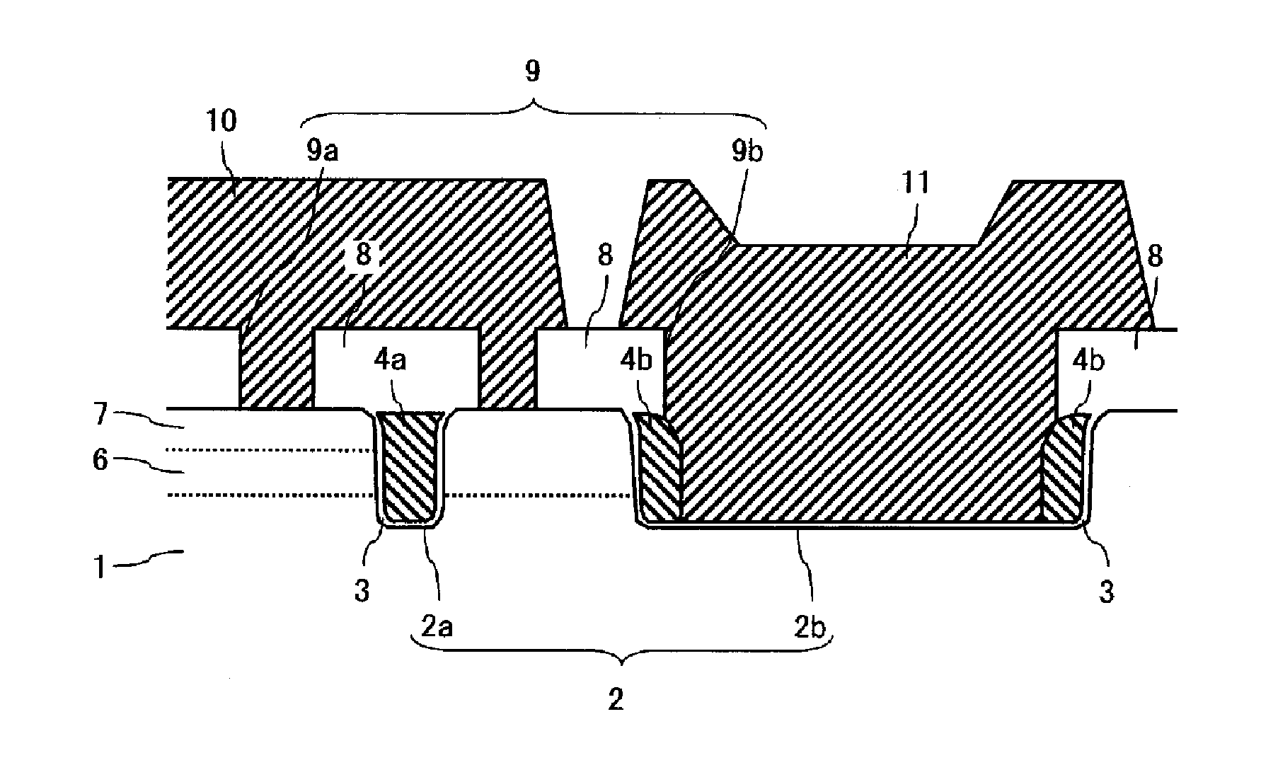
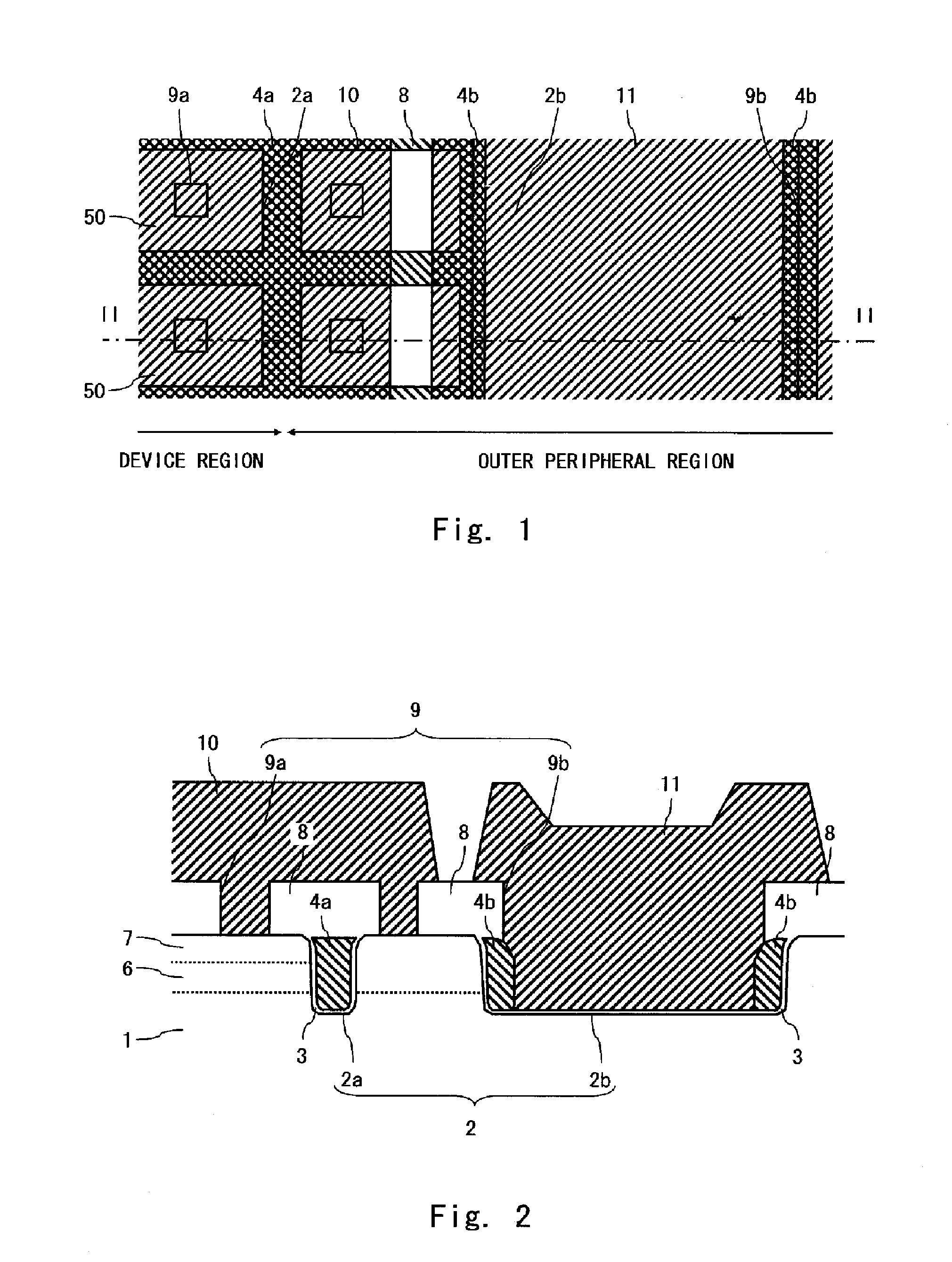
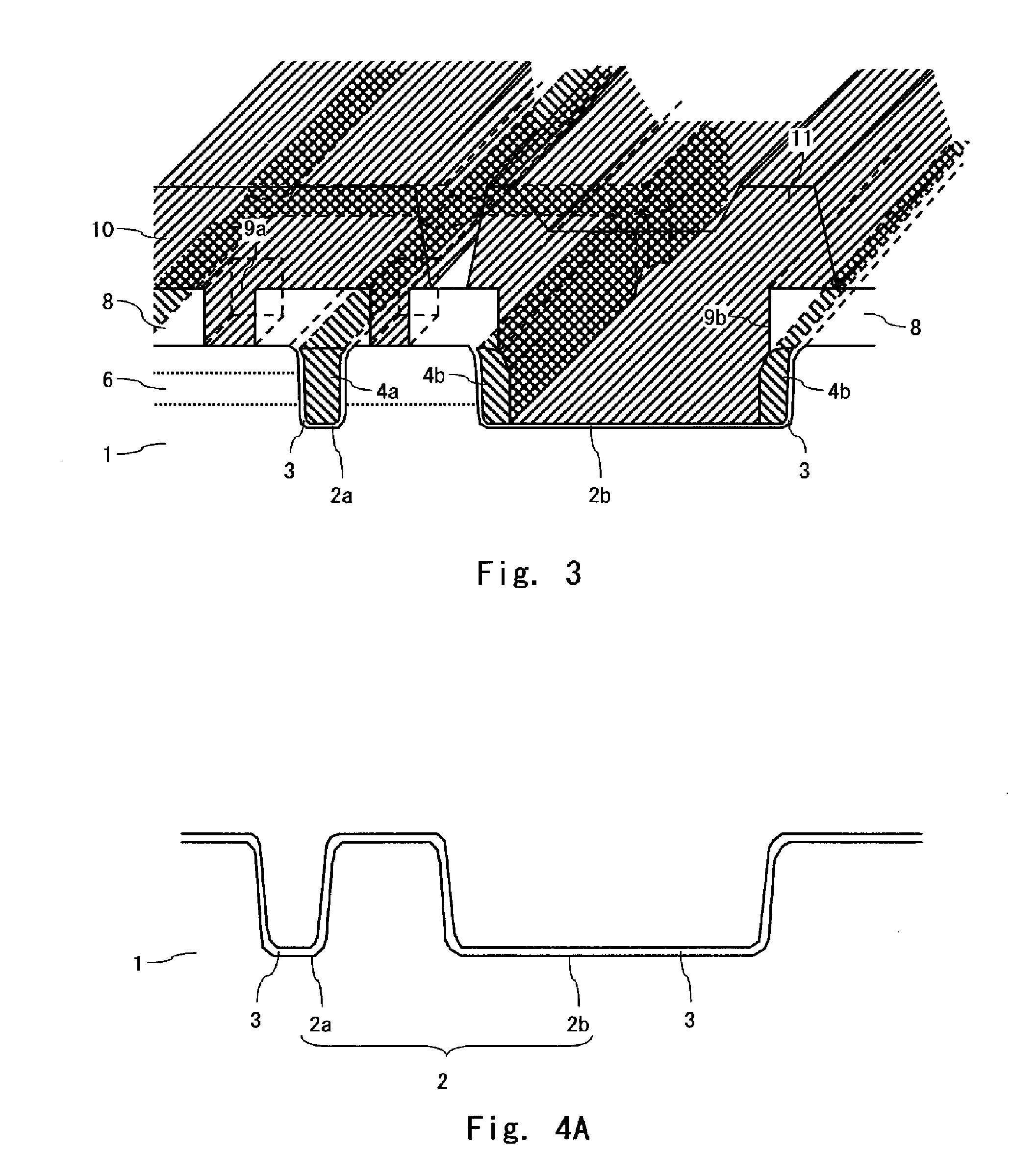
[0032]First, the configuration of a semiconductor device according to this exemplary embodiment is described with reference to FIGS. 1 to 3. FIG. 1 is a top view of the semiconductor device according to this exemplary embodiment. FIG. 2 is a cross-sectional diagram taken along the line II-II of FIG. 1. FIG. 3 is a perspective view from the cross-section II-II of FIG. 1.

[0033]The semiconductor device of this exemplary embodiment is provided with a semiconductor substrate of a first conductivity type (for example, n+ type). The semiconductor ...


PUM


Abstract

A semiconductor device according to the present invention having a vertical MOSFET that includes a first trench that is formed in a semiconductor substrate and includes a gate electrode of the vertical MOSFET embedded therein with a gate insulating film interposed therebetween, a second trench that is connected with the first trench and has a trench width wider than the first trench, a gate pad that is connected with the gate electrode and formed to a sidewall of the second trench with the gate insulating film interposed therebetween, and a gate line that is connected with a sidewall of the gate pad and electrically connects with the gate electrode via the gate pad.

Description

INCORPORATION BY REFERENCE[0001]This application is based upon and claims the benefit of priority from Japanese patent application No. 2009-097232, filed on Apr. 13, 2009, the disclosure of which is incorporated herein in its entirety by reference.BACKGROUND[0002]1. Field of the Invention[0003]The present invention relates to a semiconductor device and a method of manufacturing the same, and particularly to a semiconductor device provided with a vertical MOSFET and a method of manufacturing the same.[0004]2. Description of Related Art[0005]Generally a vertical MOSFET (UMOSFET) is used as a power device such as a power MOSFET (Metal-Oxide-Semiconductor Field-Effect Transistor) to be used as a switch for handling high current and voltage. In the vertical MOSFET, a gate electrode is provided inside a trench and a channel is formed in the vertical direction. Then, a source electrode is formed to one surface of a semiconductor substrate, a drain electrode is formed to the backside of ano...

Claims


Application Information

Patent Timeline
IPC IPC(8): H01L29/78H01L21/28
CPCH01L21/28132H01L21/2815H01L21/823487H01L29/0696H01L29/4236H01L29/42372H01L29/42376H01L2924/0002H01L29/4238H01L29/7811H01L29/7813H01L2924/00
Inventor KANEKO, ATSUSHI
Owner RENESAS ELECTRONICS CORP
Why Eureka
Try Eureka