OLED display panel and manufacture method thereof

Inactive Publication Date: 2018-07-12
WUHAN CHINA STAR OPTOELECTRONICS TECH CO LTD
View PDF5 Cites 2 Cited by
  • Summary
  • Abstract
  • Description
  • Claims
  • Application Information

AI Technical Summary

Benefits of technology

The present invention provides a method for manufacturing an OLED display panel that prevents interference between neighboring sub pixels, resulting in higher color purity and better color washout. This is achieved by creating a surface with diffuse reflection roughness on the inorganic layer in the thin film package layer corresponding to the non-pixel areas. The light emitted by each sub pixel is diffused and reflected as incident into the non-pixel areas, resulting in a less intense reflection and reduced interference. This method produces a high-quality OLED display panel with improved color purity and washout.

Problems solved by technology

As shown in FIG. 1, because the flexible OLED display panel will be frequently in a bent state, the phenomenon that a portion of light ultimately outgoes from the adjacent sub pixel occurs after the light emitted by the OLED light emitting layer 100 of one sub pixel is reflected and / or refracted in the package layer 200, and then interferes the outgoing light of the adjacent sub pixels, and leads to the color purity decrease of the single sub pixel, and the color washout issue appeared for the entire flexible OLED display panel to influence the display result.

Method used


Image

  • OLED display panel and manufacture method thereof
  • OLED display panel and manufacture method thereof
  • OLED display panel and manufacture method thereof

Examples


Embodiment Construction

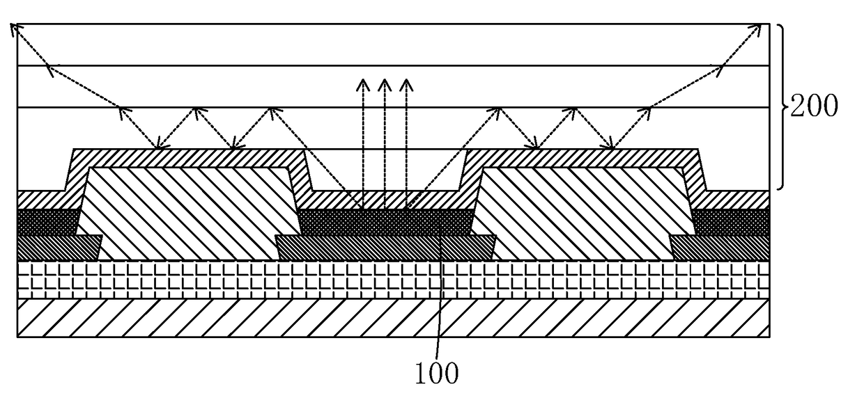
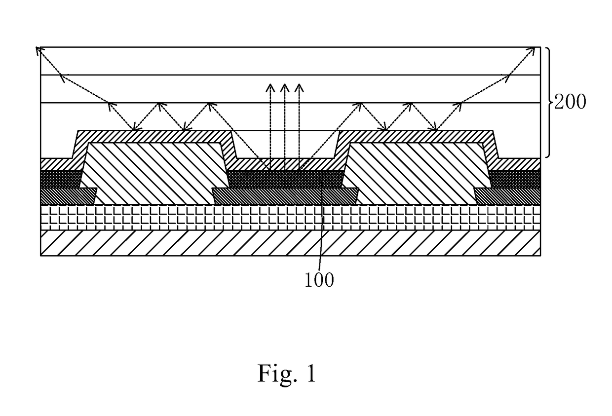
[0052]For better explaining the technical solution and the effect of the present invention, the present invention will be further described in detail with the accompanying drawings and the specific embodiments.

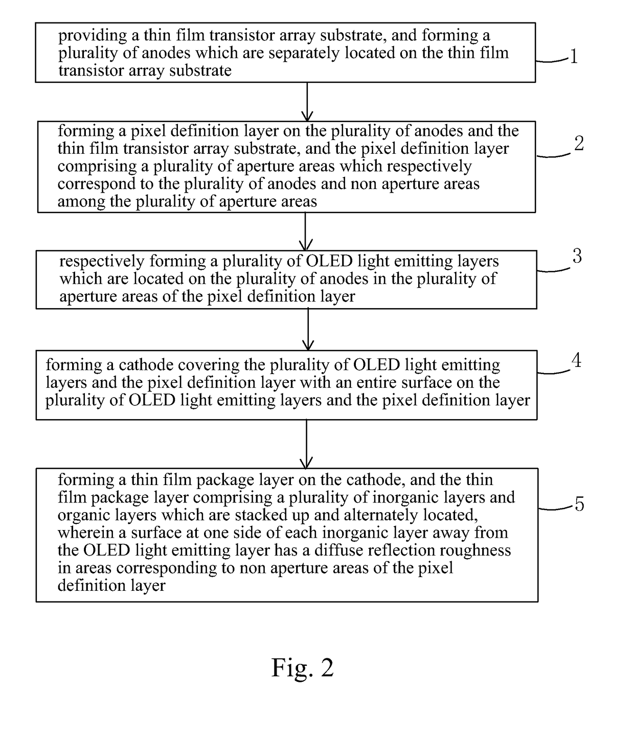
[0053]Please refer to FIG. 2. The present invention provides a manufacture method of an OLED display panel, comprising steps of:[0054]step 1, as shown in FIG. 3, providing a thin film transistor array substrate 10, and forming a plurality of anodes 20 which are separately located on the thin film transistor array substrate 10.

[0055]Specifically, the thin film transistor array substrate 10 comprises a substrate 11 and a thin film transistor array layer 12 located on the substrate 11.

[0056]Specifically, the substrate 11 can be a rigid substrate or a flexible substrate. The rigid substrate is preferably to be a glass substrate, and the flexible substrate is preferably to be a polyimide layer.

[0057]As the substrate 11 is a rigid substrate, the OLED display panel manufactured there...


PUM


Abstract

The present invention provides an OLED display panel and a manufacture method thereof. In the manufacture method of the OLED display panel of the present invention, by using the method of plasma bombardment to make a surface of the inorganic layer in the thin film package layer corresponding to the areas of the non pixel areas have a diffuse reflection roughness so that the light emitted by the OLED light emitting layer of the each sub pixel will be diffused and reflected as being incident into the area. The light is divergent and is atomized everywhere, and cannot be intensively reflected and / or refracted, and then cannot outgo from the adjacent sub pixel. Therefore, it can prevent that the light emitted by each sub pixel interferes the adjacent sub pixels to raise the color purity of single sub pixel and to improve the color washout of the OLED display panel.

Description

FIELD OF THE INVENTION[0001]The present invention relates to a display technology field, and more particularly to an OLED display panel and a manufacture method thereof.BACKGROUND OF THE INVENTION[0002]The Organic Light Emitting Display (OLED) device possesses many outstanding properties of self-illumination, low driving voltage, high luminescence efficiency, short response time, high clarity and contrast, near 180° view angle, wide range of working temperature, applicability of flexible display and large scale full color display. The OLED is considered as the most potential display device.[0003]The OLED can be categorized into two major types according to the driving methods, which are the Passive Matrix OLED (PMOLED) and the Active Matrix OLED (AMOLED), i.e. two types of the direct addressing and the Thin Film Transistor (TFT) matrix addressing. The AMOLED comprises pixels arranged in array and belongs to active display type, which has high lighting efficiency and is generally uti...

Claims


Application Information

Patent Timeline
IPC IPC(8): H01L51/52H01L27/32H01L51/00H01L51/56
CPCH01L51/5281H01L27/3246H01L51/0097H01L51/5218H01L51/5234H01L51/5256H01L51/56H01L51/0017H01L2227/323H01L2251/5315H01L2251/5338H10K59/00H10K50/85H10K50/856H10K71/00H10K59/35H10K59/122H10K77/111H10K50/8445H10K50/854H10K50/86H10K2102/3026H10K2102/311H10K50/818H10K50/828H10K71/231H10K59/1201
Inventor YU, WEI
Owner WUHAN CHINA STAR OPTOELECTRONICS TECH CO LTD
Why Eureka
Try Eureka