
Display panel and electronic device comprising thereof
a technology of electronic devices and display panels, which is applied in the field of semiconductor devices to achieve the effects of less affected image sensing capability of display panels, thinner thickness of display panels, and lighter weight of display panels
- Summary
- Abstract
- Description
- Claims
- Application Information
AI Technical Summary
Benefits of technology
Problems solved by technology
Method used
Image

Examples
first embodiment
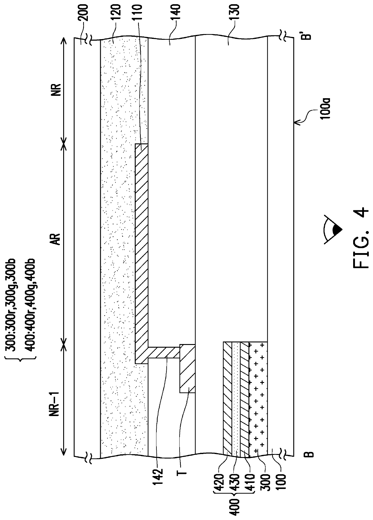
[0044]FIG. 6 is a schematic cross-sectional view of a sub-pixel in another embodiment of the display panel in FIG. 2 taken along line B-B′. It should be indicated that the embodiment of FIG. 6 adopts the reference numeral and partial content of the embodiment of FIG. 4, wherein the same or similar reference numeral represents the same or similar element, and the same technical content is omitted. The omitted descriptions can be derived from the embodiments and effects described above and thus no repetition is incorporated hereinafter.
[0045]Referring to FIG. 6, in the embodiment shown in FIG. 6, the color conversion element 300r, 300g and 300b may be a plurality of wire grids substantially parallel with each other and may be a single-layer structure or a multi-layer structure, and the material thereof may be metal, alloy, the inorganic material described above, the original material described above, or other suitable material. When the color conversion elements 300r, 300g and 300b ar...
second embodiment
[0055]FIG. 10 is a schematic cross-sectional view of a sub-pixel in another embodiment of the display panel in FIG. 2 taken along line B-B′. It should be indicated that, the embodiment of FIG. 10 adopts the reference numeral and partial content of the embodiment of FIG. 9, wherein the same or similar reference numerals represent the same or similar elements, and the same technical content is omitted. The omitted descriptions can be derived from the embodiments and effects described above and thus no repetition is incorporated hereinafter.
[0056]Referring to FIG. 10, the main difference between the embodiment of FIG. 10 and the embodiment of FIG. 9 is that the color conversion elements 300r, 300g and 300b may be a plurality of wire grids substantially parallel with each other, and the property and effect of the wire grids can be derived from the above-mentioned embodiments (e.g., embodiment of FIG. 6); therefore, no repetition is incorporated hereinafter. In the embodiment, the outer ...
PUM
 Abstract
Description
Claims
Application Information