Multi-display device and display modules

a multi-display and display module technology, applied in the field of multi-display devices, can solve the problems of affecting the appearance of liquid crystal modules, affecting the display quality, and affecting the display quality, and achieve the effects of simple configuration, less conspicuous image modulation elements, and increased cos

Inactive Publication Date: 2015-01-15
TOUOKU UNIVERISTY
View PDF21 Cites 7 Cited by
  • Summary
  • Abstract
  • Description
  • Claims
  • Application Information

AI Technical Summary

Benefits of technology

[0021]The multi-display device of the present invention brings about a remarkable effect of eliminating the use of conventional means (such as upright imaging means) that would invite cost increases and of, with a simple configuration, making the seams between image modulation elements less conspicuous and giving a satisfactory feeling of resolution.

Problems solved by technology

However, the seams between liquid crystal modules arranged in such a tiling manner are problematically so conspicuous as to lower display quality.
However, the technology disclosed in Patent Literature 1 presents the following problem: Since the frame of each of the liquid crystal panels is narrower than the pitch between pixels, the frame area is extremely narrow, with the result that the liquid crystal panel is susceptible to the influence of its external environment and may therefore easily cause a display defect.
Further, the technology disclosed in Patent Literature 2 presents various problems due to the use of organic LEDs.
That is, the cost rises simply as much as the organic LEDs are arranged.
Further, unless the liquid crystal panels and the organic LEDs are matched in display quality (luminance, chromaticity, etc.), there will be a dramatic reduction in image display quality.
Furthermore, unless the display life of the organic LEDs is equal in performance to the liquid crystal panels, there will be a reduction in image display quality due to change over time.

Method used


Image

  • Multi-display device and display modules
  • Multi-display device and display modules
  • Multi-display device and display modules

Examples


embodiment 1

[0033]An embodiment of the present invention is described below.

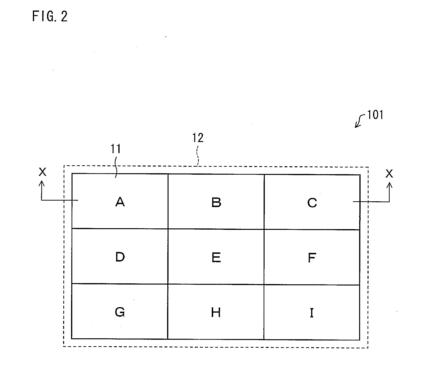
[0034]FIG. 2 shows a plan view of a multi-display device 101 according to the present embodiment.

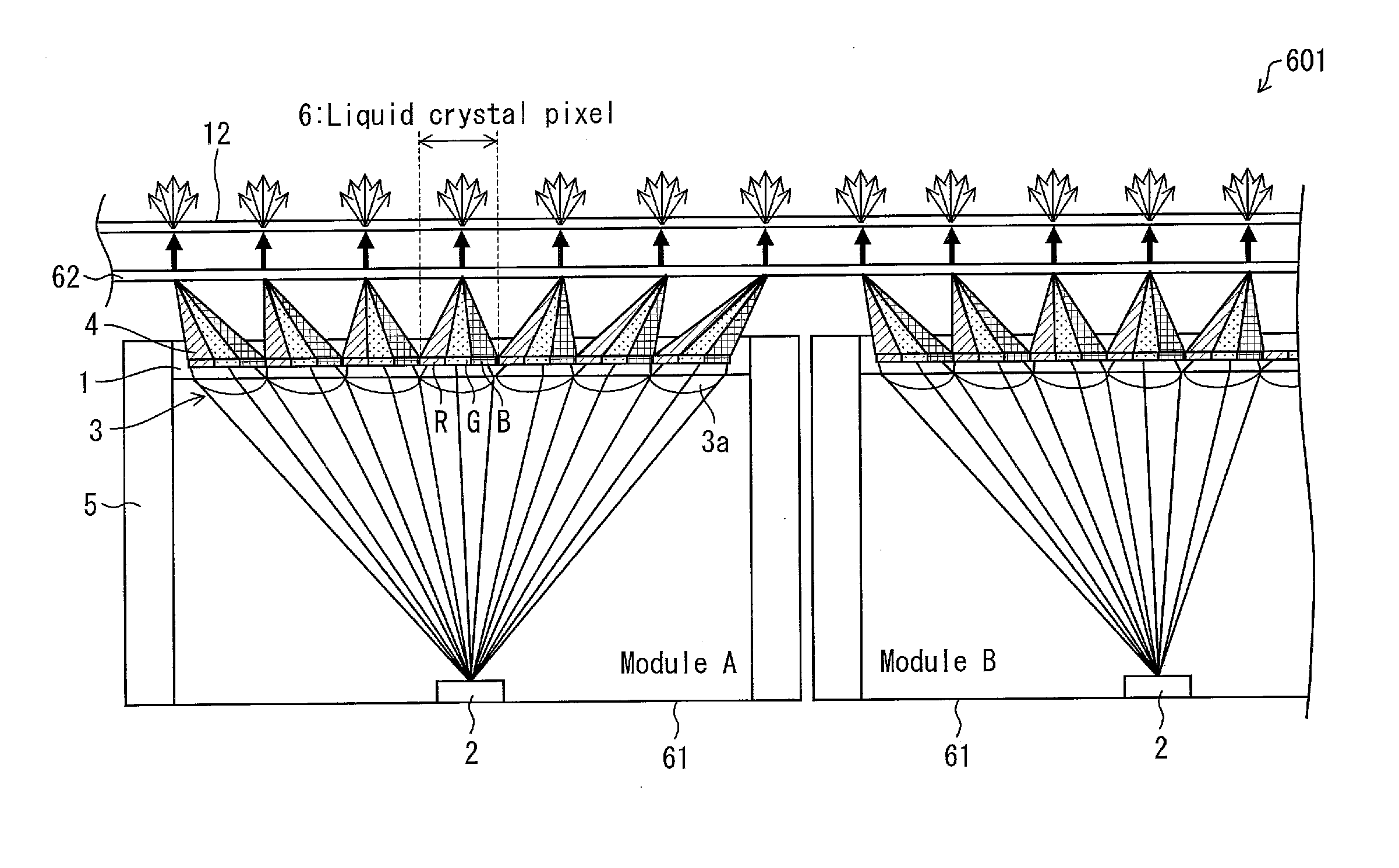
[0035]The multi-display device 101 achieves a large-screen display by having a parallel and tiling arrangement of liquid crystal modules (display modules) 11 as shown in FIG. 2. The liquid crystal modules, arranged in such a tiling manner, are covered with a diffuser panel 12 (diffusing element) that functions as a screen. This allows images from the liquid crystal modules 11 to be projected onto the diffuser panel 12 and joined to each other on a diffusing surface of the diffuser panel 12, thus achieving a large-screen display.

[0036]Normally, in the case of a large-screen display carried out by a tiling arrangement of liquid crystal modules 11, those regions on the screen being displayed which correspond to the seams between the liquid crystal modules 11 are problematically so conspicuous as to lower display quality.

[0037]I...

embodiment 2

[0077]Another embodiment of the present invention is described below.

[0078]FIG. 3 shows a schematic cross-sectional view of a liquid crystal module 21 constituting a multi-display device 201 according to the present embodiment.

[0079]As shown in FIG. 3, the liquid crystal module 21 is constituted by a parallel arrangement of light source sections 2 in a plurality of blocks 21a. That is, the liquid crystal module 21 is constituted by dividing a single liquid crystal module 21 into a plurality of units each of which serves as a block 21a and providing a single light source section 2 in each of the blocks 21a.

[0080](Details of the Blocks 21a)

[0081]The light source section 2 in each block 21a is located directly below substantially the central part of a portion of the display screen for which that block 21 is responsible. The light source sections 2 are identical in configuration to that of Embodiment 1, and as such, they are not described here. For convenience of explanation, the block...

embodiment 3

[0105]Still another embodiment of the present invention is described below. The present embodiment describes an example where each light source section is constituted by three colors of LED, namely RGB LEDs, whereas each of the light source sections 2 employed in Embodiment 1 is a white LED.

[0106]FIG. 5 shows a schematic cross-sectional view of liquid crystal modules 31 constituting a multi-display device 301 according to the present embodiment.

[0107](Details of the Liquid Crystal Modules 31)

[0108]As shown in FIG. 5, each of the liquid crystal modules 31 has a light source section 32 located directly below substantially the central part of the display screen of the liquid crystal panel 1, as with the liquid crystal modules 11 of Embodiment 1. It should be noted here that the light source section 32 is constituted by LED light sources that emit RGB colors of light, respectively. These LED light sources are placed at spaces from one another. This allows rays of light that are emitted ...


PUM


Abstract

A multi-display device (101) of the present invention includes fry-eye lens arrays (3), located between a plurality of liquid crystal modules (11) arranged in parallel and in a tiling manner and a diffusing element (12), which cause rays of light emitted from light source sections (2) and transmitted through the liquid crystal modules (11) to be condensed on the diffusing element (12) at a pitch that is wider than a pixel pitch of the liquid crystal modules (11). This makes it possible with a simple configuration to make seams between image modulation elements less conspicuous and give a satisfactory feeling of resolution.

Description

TECHNICAL FIELD[0001]The present invention relates to a multi-display device that makes a large-screen display possible by having a tiling arrangement of liquid crystal modules.BACKGROUND ART[0002]Currently, an extra-large screen display such as digital signage is achieved by a tiling arrangement of liquid crystal modules.[0003]However, the seams between liquid crystal modules arranged in such a tiling manner are problematically so conspicuous as to lower display quality.[0004]In order to solve this problem, technologies of making the seams between liquid crystal modules inconspicuous have been proposed.[0005]For example, Patent Literature 1 discloses a technology of, with use of a precision cutting technique in the step of cutting seams in the process for manufacturing liquid crystal panels, making the seams between the liquid crystal panels less conspicuous by arranging the liquid crystal panels so that spaces between them are nearly as narrow as those between pixels.[0006]Further...

Claims


Application Information

Patent Timeline
Patent Type & Authority Applications(United States)
IPC IPC(8): G06F3/14
CPCG06F3/1446H04N9/3147G09F9/30G09F9/35H04N9/12
Inventor UCHIDA, TATSUOSUZUKI, YOSHITOKAWAKAMI, TOHRUSEKIYA, KAZUONISHIZAWA, MASAHIROISHINABE, TAKAHIROEHARA, KATSUNORIHASHIMOTO, YOSHIHIROITOH, YASUHISAYAMAMOTO, YOSHITAKAISHII, YUTAKA
Owner TOUOKU UNIVERISTY
Why Eureka
Try Eureka