Manufacturing method of image forming apparatus, manufacturing apparatus of image forming apparatus, image forming apparatus, manufacturing method of panel apparatus, and manufacturing apparatus of panel apparatus

a manufacturing method and technology of image forming apparatus, applied in the manufacture of cold cathode, electric discharge tube/lamp, electric discharge system, etc., can solve the problem of low vacuum degree in the apparatus, inability to obtain the vacuum degree necessary for stable electron emission characteristics, and pressure fluctuation

Inactive Publication Date: 2001-07-03
CANON KK
View PDF19 Cites 68 Cited by
  • Summary
  • Abstract
  • Description
  • Claims
  • Application Information

AI Technical Summary

Problems solved by technology

However, in the image forming apparatus using the above conventional electron emitting device, there is a case where the following problems occur.
However, since the distance between the electron source substrate and the face plate is short and the conductance of the gas is small, in an exhausting step in the image forming apparatus subsequent to the seal bonding step, it takes time to exhaust the space to an adequate degree of vacuum through an exhaust pipe or, if the exhausting step is finished in a short time, the degree of vacuum in the apparatus is low, or a pressure fluctuation occurs.
There is, consequently, a case where a degree of vacuum which is necessary for stable electron emitting characteristics cannot be obtained.
Although a high positioning precision is required in the relative arrangement between the electron emitting device and the fluorescent body in order to prevent a color deviation or the like, there is a case where the necessa

Method used


Image

  • Manufacturing method of image forming apparatus, manufacturing apparatus of image forming apparatus, image forming apparatus, manufacturing method of panel apparatus, and manufacturing apparatus of panel apparatus
  • Manufacturing method of image forming apparatus, manufacturing apparatus of image forming apparatus, image forming apparatus, manufacturing method of panel apparatus, and manufacturing apparatus of panel apparatus
  • Manufacturing method of image forming apparatus, manufacturing apparatus of image forming apparatus, image forming apparatus, manufacturing method of panel apparatus, and manufacturing apparatus of panel apparatus

Examples


embodiment 1

[Embodiment 1]

In the first embodiment of the invention, an image forming apparatus with a construction shown in FIG. 6 is manufactured. In the embodiment, a plurality of surface conducting type electron emitting devices serving as cold cathode electron emitting devices are formed as electron emitting devices on the rear plate. A fluorescent body is attached on the face plate. A color image forming apparatus having an aspect ratio of 4:3 in which a valid display area has a diagonal line of 15 inches is formed. First, the image forming apparatus of the invention will be described with reference to FIG. 6 and its manufacturing method will be subsequently described with reference to FIG. 2 showing a manufacturing flow together with FIGS. 1A to 1C.

FIG. 6 is a perspective view of the image forming apparatus used in this embodiment, and a part of a panel is cut away to show an internal structure.

In the diagram, reference numeral 65 denotes a rear plate; 66 a supporting frame; and 67 a face...

embodiment 2

[Embodiment 2]

The second embodiment of the invention relates to an image forming apparatus using the field emitting device as a kind of cold cathode electron emitting devices and relates to a case where a spacer is attached as an atmospheric pressure proofing member in order to realize a light weight.

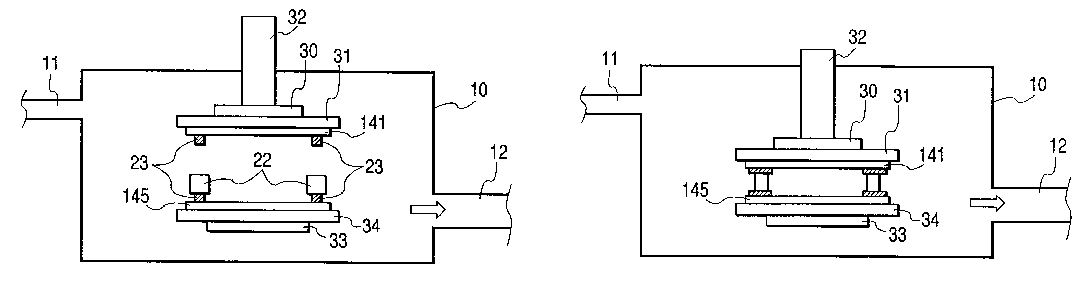
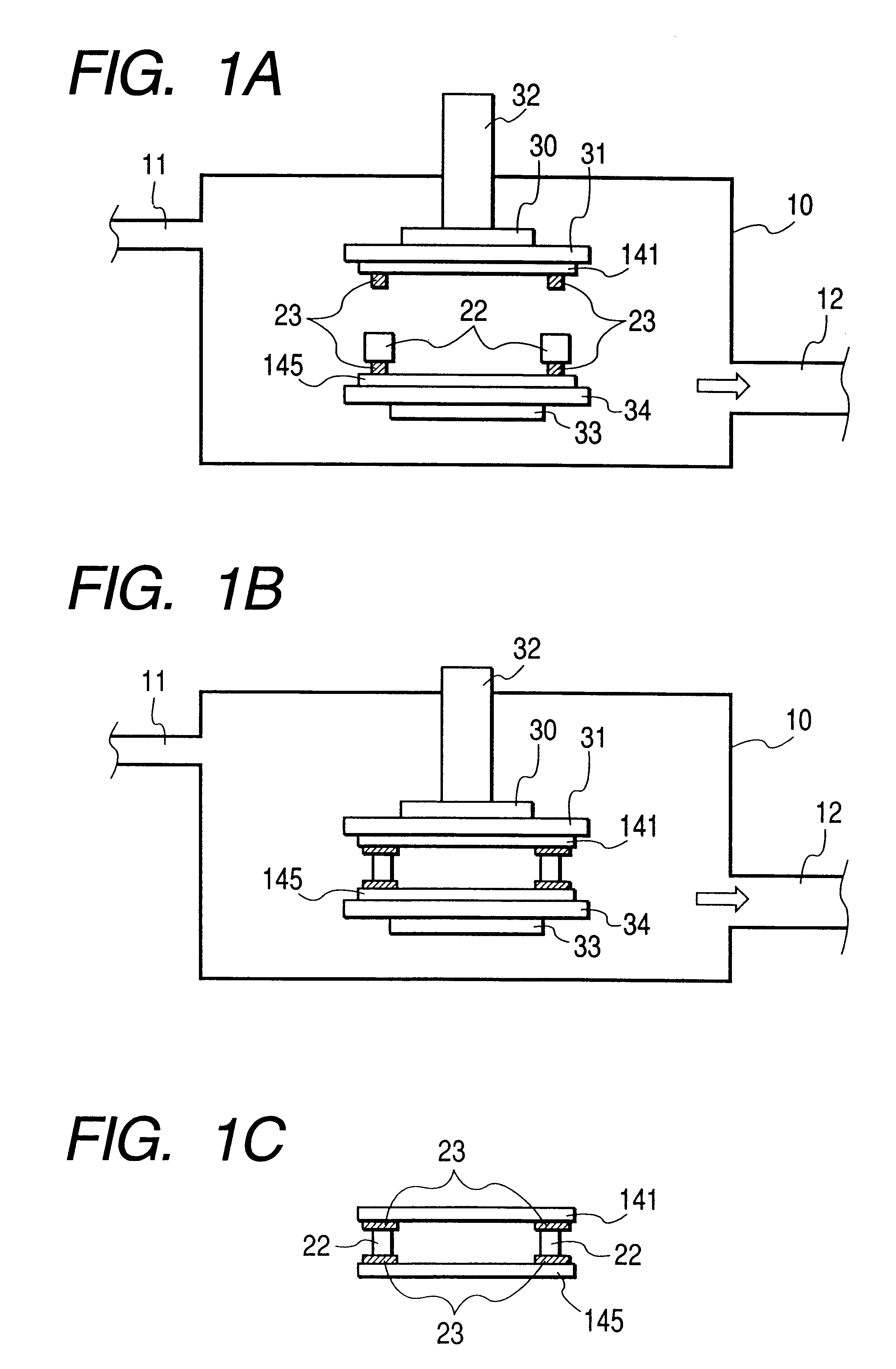
First, the field emitting device will be described with reference to FIGS. 9A and 9B and an image forming apparatus using the field emitting device will be explained with reference to FIGS. 10A and 10B. In FIGS. 9A and 9B, reference numeral 131 denotes a rear plate; 132 a face plate; 133 a cathode; 134 a gate electrode; 135 an insulating layer between the gate and the cathode; 136 a focusing electrode; and 138 an insulating layer between the gate and the focusing electrode. In FIGS. 10A and 10B, reference numeral 141 denotes a face plate; 143 a supporting frame; 145 the rear plate; and 147 a spacer.

A size of valid display area of the image forming apparatus has an aspect ratio of 4:3 an...

embodiment 3

[Embodiment 3]

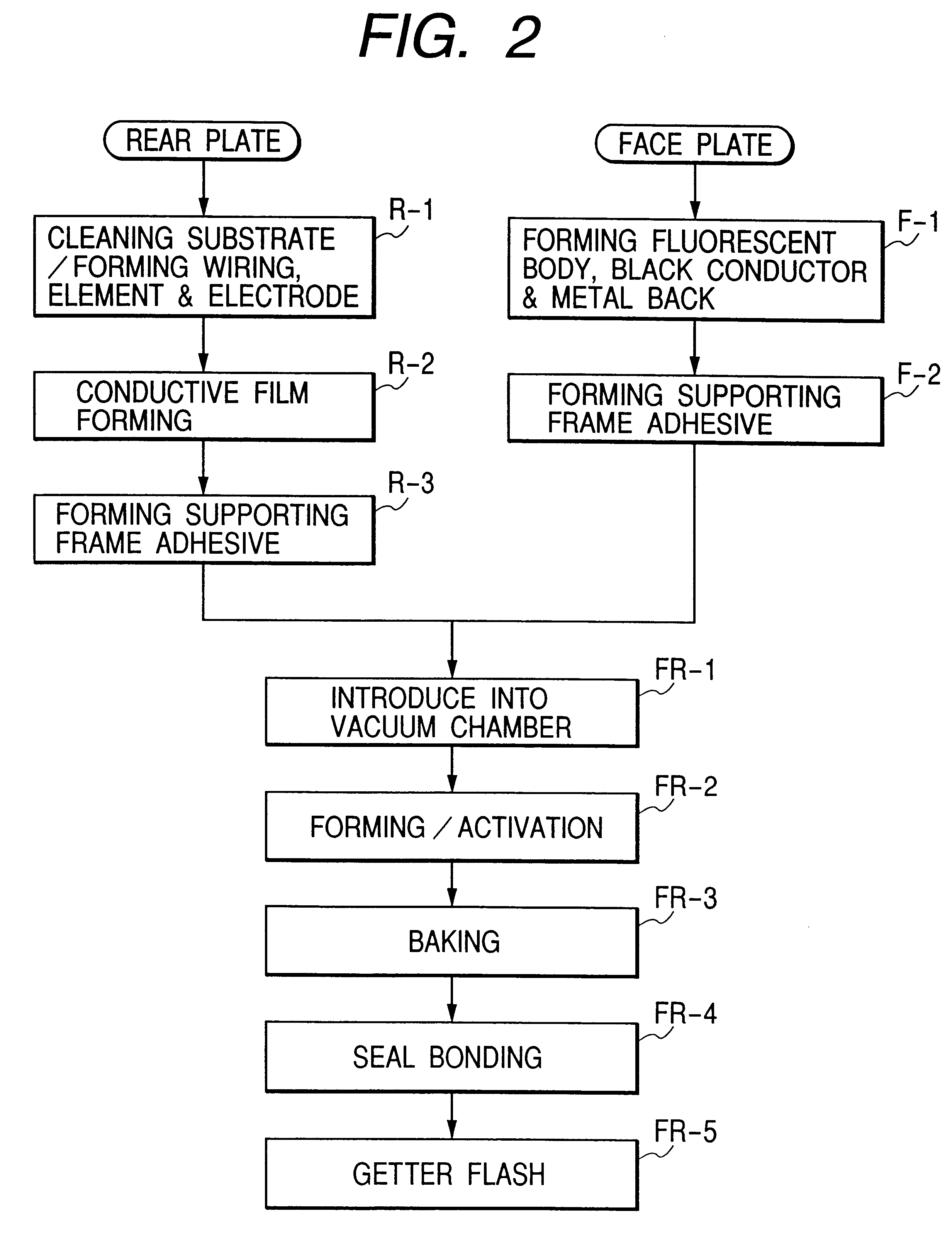
The embodiment relates to an example of a manufacturing apparatus of the image forming apparatus using the surface conducting type electron emitting device and will be explained hereinbelow with reference to a flowchart of FIG. 4 and an apparatus schematic diagram of FIG. 5. First, the apparatus will be explained.

In the manufacturing apparatus of the embodiment, reference numeral 10 denotes the load locking type vacuum chamber; 42 an oil-free evacuating apparatus; 39 a gas cylinder which is used in the activating step; 37 a voltage source which is used in the forming and activating steps; 34 the rear plate heating apparatus; 34' a face plate heating apparatus; 30 and 33 the position fine adjusting mechanisms of the rear plate and the face plate; 32 the mechanism for moving the face plate or rear plate in the Z-axis direction and pressing the face plate and the rear plate; 36 CCDs serving as detecting means for observing positions of position matching patterns (alignmen...


PUM

PropertyMeasurementUnit
Temperatureaaaaaaaaaa
Electrical conductoraaaaaaaaaa
Heightaaaaaaaaaa

Abstract

To obtain a stable image forming apparatus of a high quality without a luminance fluctuation and a color mixture due to a positional deviation, the following construction is disclosed. A method of manufacturing an image display apparatus in which a first substrate on which fluorescent body exciting means is arranged and a second substrate on which a fluorescent body that emits light by the fluorescent body exciting means is arranged are arranged so as to face each other and are adhered through joining members at their peripheries, wherein a seal bonding step of adhering the first and second substrates through a joining members and a step of performing a position matching of the first and second substrates are executed in a vacuum.

Description

1. Field of the InventionThe invention relates to a manufacturing method of an image forming apparatus, a manufacturing apparatus of an image forming apparatus, and the image forming apparatus manufactured by the manufacturing method.2. Related Background ArtHitherto, as electron emitting devices, mainly, two kinds of devices, i.e., a device using a thermionic emitting device and a device using a cold cathode electron emitting device, has been known. As cold cathode electron emitting devices, there are a field emission type (hereinafter, abbreviated as an "FE" type), a metal / insulating layer / metal type (hereinafter, abbreviated as an "MIM" type), a surface conducting type electron emitting device, and the like.As an example of the FE type, there has been known a device disclosed in W. P. Dyke & W. W. Dolan, "Field Emission", Advances in Electron Physics, 8,89, 1956, C. A. Spindt, "Physical Properties of Thin-Film Field Emission Cathodes with Molybdenum Cones", J. Appl. Phys., 47,524...

Claims


Application Information

Patent Timeline
IPC IPC(8): H01J9/26C03C27/06H01J9/02H01J9/385H01J9/40
CPCH01J9/261H01J2329/00
Inventor NAKANISHI, KOICHIROTAKAMATSU, OSAMUTAGAWA, MASAHIROKOYAMA, SHINYAUEDA, KAZUYUKI
Owner CANON KK
Why Eureka
Try Eureka