Common electrode substrate and liquid crystal display device having the same

a liquid crystal display and common electrode technology, applied in the direction of identification means, instruments, optics, etc., can solve the problems of narrow viewing angle, low contrast, low yield, etc., and achieve the effect of good display characteristics and high luminan

Inactive Publication Date: 2005-01-04
UNIFIED INNOVATIVE TECH
View PDF10 Cites 176 Cited by
  • Summary
  • Abstract
  • Description
  • Claims
  • Application Information

AI Technical Summary

Benefits of technology

An object of the present invention is to provide a common electrode substrate capable of providing high luminance and good display characteristics as well as a liquid crystal display device having such a common electrode substrate.
The above object is attained by a common electrode substrate comprising a transparent insulating substrate to be arranged opposite to an array substrate having pixel electrodes formed in respective pixel regions that are defined by a plurality of gate bus lines and drain bus lines, and to hold a liquid crystal having negative dielectric anisotropy; a common electrode formed on the transparent insulating substrate; alignment regulating structures having linear protrusions formed on the common electrode; and a light shield film formed on the transparent insulating substrate and having overlap regions that overlap the pixel electrodes when viewed in the direction perpendicular to the surface of the transparent insulating substrate so as to shield, from light, alignment defective regions of the liquid crystal formed in regions of end portions of the pixel electrodes.

Problems solved by technology

While TN mode liquid crystal display devices have such advantages that they can be made thin, they have a first disadvantage of a narrow viewing angle and a second disadvantage of low contrast.
Failures due to pollution and static electricity that occur during the rubbing are factors of lowering the yield.
Although the MVA liquid crystal display device provides a wide viewing angle, it had a problem that there exist regions where the alignment of liquid crystal molecules is not stable, resulting in lowering the luminance.
As described above, the conventional MVA liquid crystal display device of FIG. 25 has the problem that when a black vertical band is displayed against a white background, a region displaying white under the black vertical band is displayed darker than the other region displaying white.
As described above, the conventional MVA liquid crystal display device of FIG. 25 has the problem that when a white vertical band is displayed against a black background, a region displaying black under the white vertical band is displayed brighter than the other region displaying black.

Method used


Image

  • Common electrode substrate and liquid crystal display device having the same
  • Common electrode substrate and liquid crystal display device having the same
  • Common electrode substrate and liquid crystal display device having the same

Examples


first embodiment

FIG. 13 is a plan view showing the configurations of the common electrode substrate and the liquid crystal display device having the substrate according to the FIG. 13 shows one pixel of the liquid crystal display device. The gate bus lines 42 extending in the right-left direction in FIG. 13 and the drain bus lines 36 extending in the top-bottom direction in FIG. 13 are formed on the array substrate 32 that is provided with the TFTs 2. Each TFT 2 is composed of a drain electrode 52 that extends from the drain bus line 42, a source electrode 54 that is arranged opposite to the drain electrode 52, and a portion (gate electrode) of the gate bus line 36 which overlaps with the drain electrode 52 and the source electrode 54. Although not shown in FIG. 13, channel layers that are amorphous silicon (α-Si) films, for example, are formed on the respective gate bus lines 36. The pixel electrodes 16 that are connected to the respective source electrodes 54 are further formed on the array subs...

second embodiment

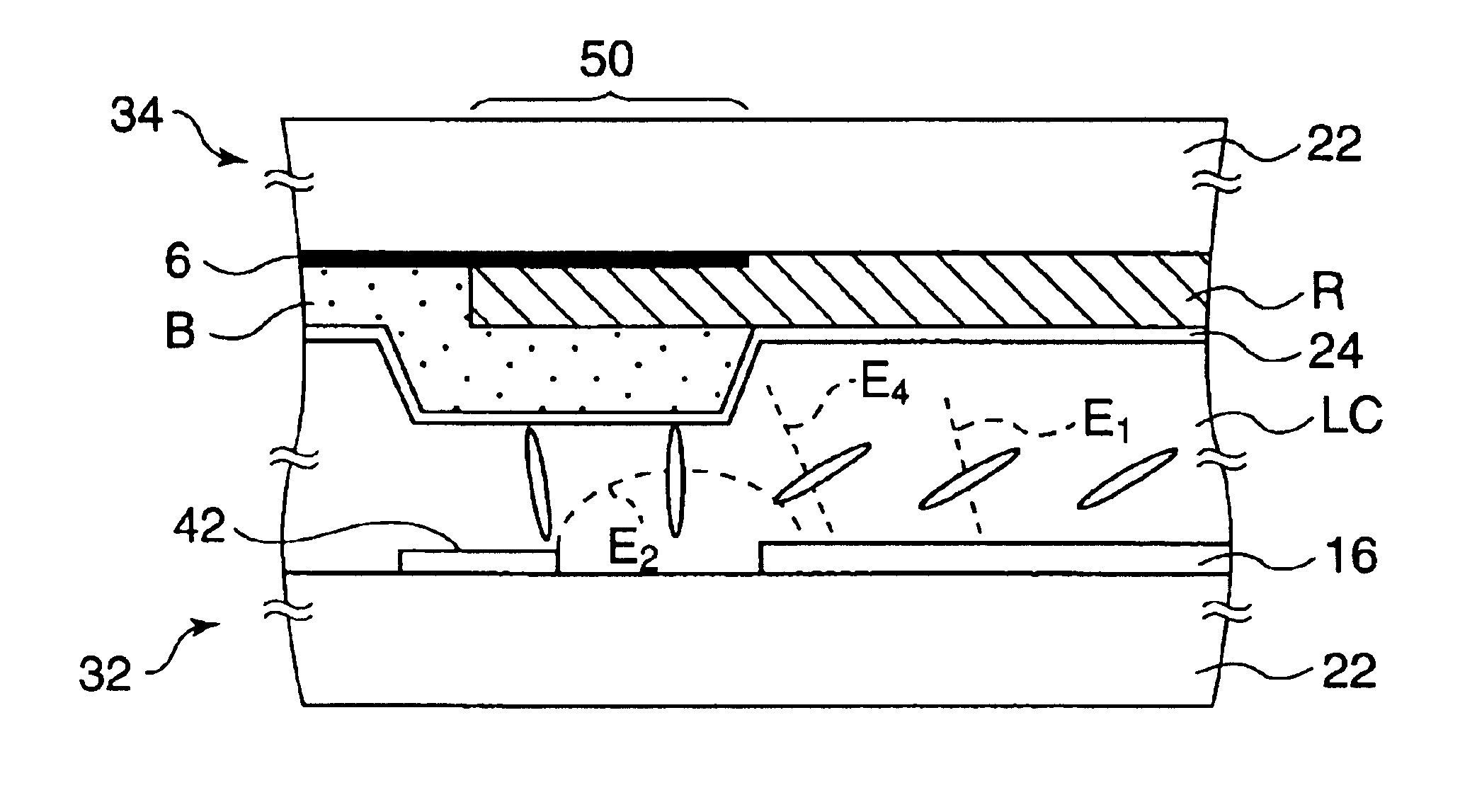
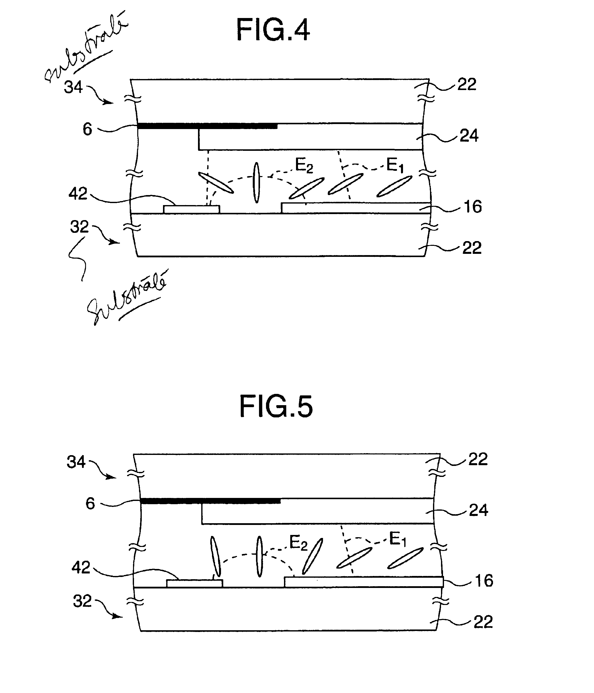
Next, the states of liquid crystal molecules in the common electrode substrate and in the liquid crystal display device having the substrate will be described with reference to FIG. 20. FIG. 20 is a simplified sectional view taken along line F—F in FIG. 19 and shows pixel in FIG. 26. The drain bus line 42 on the left side is formed on the array substrate 32, and the pixel electrode 16 is formed on the right side on the array substrate 32 (see FIG. 20). On the other hand, on the common electrode substrate 34, the light shield film 6 is formed in the region other than the region that is opposed to the pixel electrode 16. The color filters R and B are formed on the common electrode substrate 34. The color filters B and R are formed in an overlap state in the resin double-layer portion 50, whereby a step is formed in the region that is opposed to the region between the pixel electrode 16 and the drain bus line 42. The common electrode 24 is formed on the color filters R and B and the e...


PUM

PropertyMeasurementUnit
widthaaaaaaaaaa
diagonal sizeaaaaaaaaaa

Abstract

A common electrode substrate has a transparent insulating substrate to be arranged opposite to an array substrate having pixel electrodes formed in respective pixel regions that are defined by a plurality of gate bus lines and drain bus lines. The substrate holds a liquid crystal having negative dielectric anisotropy. A common electrode is formed on the transparent insulating substrate; alignment regulating structures having linear protrusions are formed on the common electrode; and a light shield film is formed on the transparent insulating substrate with overlap regions that overlap the pixel electrodes when viewed in the direction perpendicular to a surface of the transparent insulating substrate, so as to shield, from light, alignment defective regions of the liquid crystal formed in regions of end portions of the pixel electrodes.

Description

BACKGROUND OF THE INVENTION1. Field of the InventionThe present invention relates to a common electrode substrate that is opposed to an array substrate as well as to a liquid crystal display device having the substrate.2. Description of the Related ArtLiquid crystal display devices have a liquid crystal that is sealed between a pair of substrates. Each of the paired substrates has at least one electrode and an alignment film. TN (twisted nematic) mode liquid crystal display devices, which are widely used conventionally, have horizontal alignment films and a liquid crystal having positive dielectric anisotropy. Liquid crystal molecules are aligned approximately parallel with the horizontal alignment film when a voltage is applied. Liquid crystal molecules rise so as to become approximately perpendicular to the horizontal alignment film when a voltage is applied to those.While TN mode liquid crystal display devices have such advantages that they can be made thin, they have a first dis...

Claims


Application Information

Patent Timeline
Patent Type & Authority Patents(United States)
IPC IPC(8): G02F1/139G02F1/1333G02F1/13G02F1/1335G02F1/1337G02F1/136G02F1/1368G09F9/30
CPCG02F1/1393G02F1/133707G02F1/133512G02F1/1337
Inventor TANIGUCHI, YOJIINOUE, HIROYASU
Owner UNIFIED INNOVATIVE TECH
Why Eureka
Try Eureka