Apparatus for driving light emitting element and system for driving light emitting element

a technology of light emitting elements and driving apparatuses, which is applied in the direction of laser optical resonator construction, laser details, printing, etc., can solve the problems of difficult integration of circuits and increased power consumption of driving apparatuses, and achieve the effect of higher modulation speed

Inactive Publication Date: 2009-05-05
FUJIFILM BUSINESS INNOVATION CORP
View PDF51 Cites 4 Cited by
  • Summary
  • Abstract
  • Description
  • Claims
  • Application Information

AI Technical Summary

Benefits of technology

[0027]Furthermore, a current flowing through the voltage source is established to be smaller than a current flowing through the light emitting element. With this construction, where high speed drive is achieved by the current flowing through the voltage source being smaller than the current flowing through the light emitting element, the power consumption can be suppressed low in the voltage source, and the entire power consumption of the driving apparatus can be achieved, and the circuit integration thereof can be facilitated. In this connection, if an attempt is made to achieve high speed drive in the case where drive using an emitter follower (or a source follower) is taken into consideration, a greater current than the current flowing through the light emitting element must be caused to flow into a transistor of the emitter follower, wherein the power consumption of the driving apparatus will be increased, and integration of circuits will be made difficult.
[0057]The apparatus for driving a light emitting element according to the twenty-ninth aspect of the invention is constructed, in addition to the apparatus for driving a light emitting element, which is described in the eighteenth, nineteenth, or twenty-sixth aspects, so that the input side and output side retaining sections are capacitors. In the apparatus for driving a light emitting element thus constructed, since the capacitor is a single element, configuration of the circuits can be remarkably facilitated by employing the capacitor as a retaining section.

Problems solved by technology

In this connection, if an attempt is made to achieve high speed drive in the case where drive using an emitter follower (or a source follower) is taken into consideration, a greater current than the current flowing through the light emitting element must be caused to flow into a transistor of the emitter follower, wherein the power consumption of the driving apparatus will be increased, and integration of circuits will be made difficult.

Method used


Image

  • Apparatus for driving light emitting element and system for driving light emitting element
  • Apparatus for driving light emitting element and system for driving light emitting element
  • Apparatus for driving light emitting element and system for driving light emitting element

Examples


embodiment 1

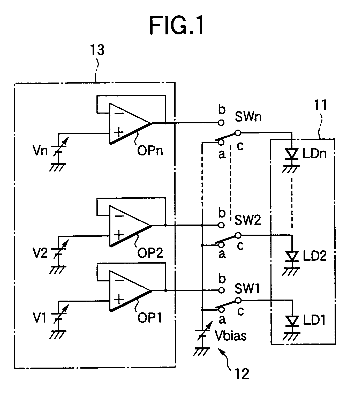
[0117]FIG. 8 is a circuit diagram showing a configurational example of a driving system using an apparatus for driving a light emitting element according to the first embodiment of the invention, for example, a surface emitting laser driving apparatus. In the present embodiment, a surface emitting laser 21 having, for example, thirty-six light emitting parts LD1 through LD36 is used as a light emitting element that is a subject to be driven.

[0118]The system for driving a surface emitting laser according to the embodiment includes a first voltage source 22 for generating a bias voltage Vbias, a second voltage source (variable voltage source) 23 for generating a drive voltage (control voltage), and an power detecting circuit 24 for detecting the power of the surface emitting laser 21. The first voltage source 22 and the second voltage source 23, respectively, correspond to the first voltage source 12 in FIG. 1 and the second voltage source 13 therein.

[0119]The bias voltage Vbias that ...

embodiment 2

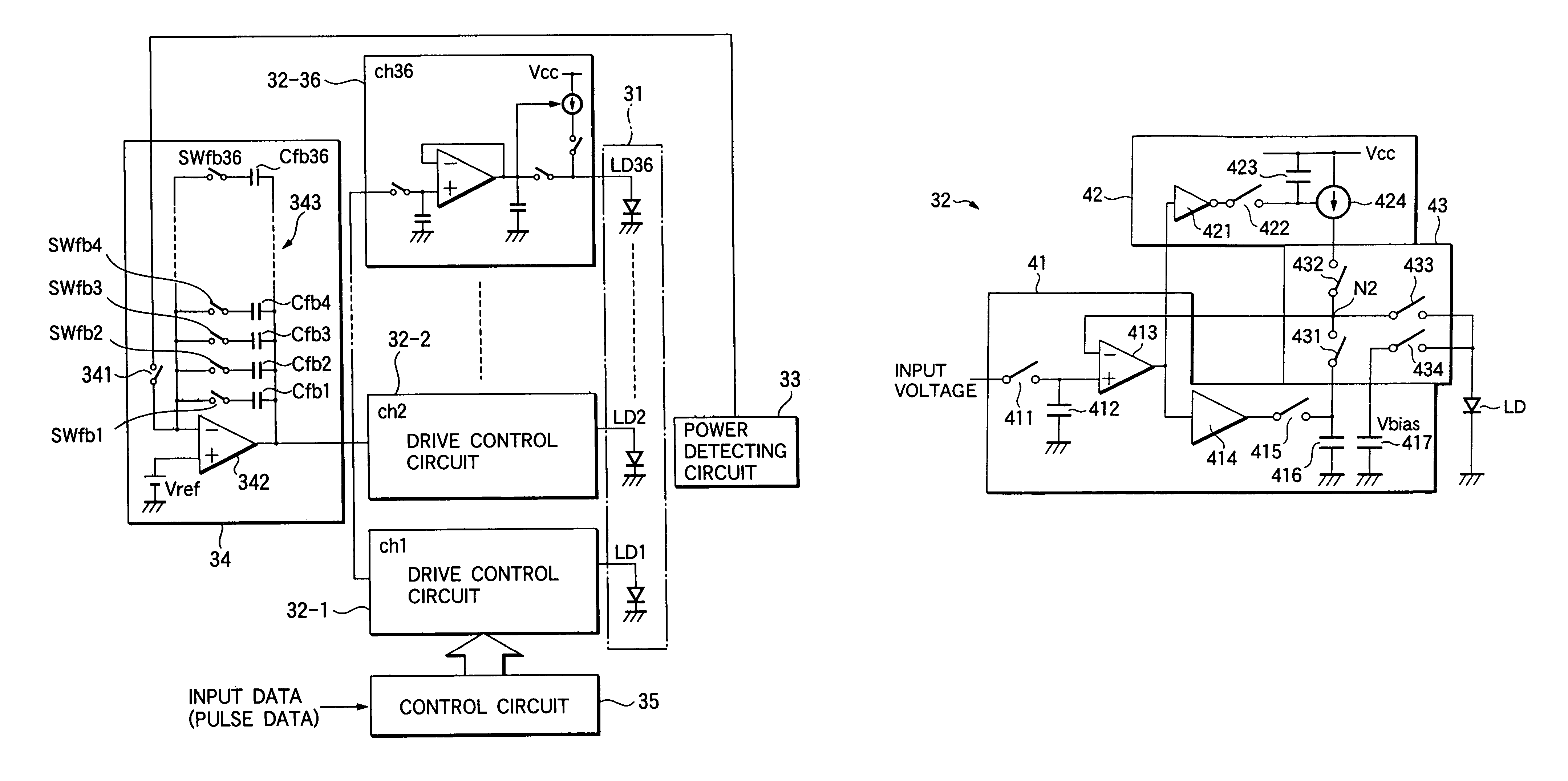
[0171]FIG. 15 is a circuit diagram showing a configurational example of an apparatus for driving a light emitting element according to the second embodiment of the present invention, a driving system in which, for example, a surface emitting laser driving apparatus is employed. In the present embodiment, a light emitting element, in which a surface emitting laser 31 having for example, 36 light emitting parts LD1 through LD36 is a subject to be driven, is used.

[0172]In FIG. 15, a surface emitting laser driving system according to the present embodiment includes drive control circuits 32-1 through 32-36 to cover 36 channels, which are provided to correspond to respective light emitting parts LD1 through LD36 of the surface emitting laser 36; a power detecting circuit 33 for detecting the power of the surface emitting laser 31; a difference amplifying circuit 34 that constitutes a feedback system for feeding detection results of the power detecting circuit 33 back to the drive control...

embodiment 3

[0208]FIG. 22 is a circuit diagram showing a configurational example of a drive control circuit of an apparatus for driving a light emitting element according to the third embodiment of the present invention, that is, for example, a surface emitting laser driving apparatus. In the same drawing, parts that are similar to those in FIG. 16 are given the same reference number. Also, a difference thereof from the surface emitting laser driving apparatus according to the second embodiment resides in only the construction of the drive control circuit 32. Therefore, where constructing a drive system, the construction thereof is basically the same as that in FIG. 15.

[0209]In FIG. 22, the voltage drive circuit 41 and the current drive circuit 42 are, respectively, provided with a circuit for compensating a power shift for a fluctuation ΔT in temperature. In detail, the compensation circuit of the voltage drive circuit 41 is composed of an error amplifier 418 and a sample hold circuit 419. A t...


PUM


Abstract

In case of driving each of light emitting parts of a surface emitting laser, each of light emitting parts is made to be in forward-bias state and switches appropriately change bias voltage, which is lower than laser oscillation threshold voltage, and drive voltages, which are not less than the laser oscillation threshold voltage to directly apply the changed voltage to each of drive ends of the light emitting parts. Whereby, each of light emitting parts is driven.

Description

[0001]This is a Division of application Ser. No. 10 / 090,146 filed Mar. 5, 2002. The entire disclosure of the prior application is incorporated by reference herein in its entirety.BACKGROUND OF THE INVENTION[0002]1. Field of the Invention[0003]The present invention relates to an apparatus for driving a light emitting element and a system for driving light emitting elements, which drive a light emitting element by causing a direct current to flow thereto, and in particular the invention relates to a preferred apparatus for driving a light emitting element and a preferred system for driving the same, which are used to drive a light emitting element having a large interval resistance (series resistance), represented by a surface emission type laser element.[0004]2. Description of the Related Art[0005]High resolution and high speed have been demanded in the field of laser xerography using a laser beam as a light source. There is a limitation in the speed (hereinafter called “modulation s...

Claims


Application Information

Patent Timeline
Patent Type & Authority Patents(United States)
IPC IPC(8): H01S3/00H01S5/062H01S5/042H01S5/068H01S5/0683H01S5/18
CPCH01S5/042B41J2/473H01S5/0427H01S5/06808H01S5/0683
Inventor IKEDA, CHIKAHO
Owner FUJIFILM BUSINESS INNOVATION CORP
Why Eureka
Try Eureka