Display device including optical sensor and driving method thereof

Active Publication Date: 2011-06-23
SEMICON ENERGY LAB CO LTD
View PDF99 Cites 65 Cited by
  • Summary
  • Abstract
  • Description
  • Claims
  • Application Information

AI Technical Summary

Benefits of technology

[0023]According to one embodiment of the present invention, a display de

Problems solved by technology

An increase in screen size or resolution causes an increase in wiring resistance or parasitic capacitance, which results in a decrease in display quality or an increase in power consumption of a display device.
Particularly in an active matrix display device, as the screen size increases, a variation in characteristics such a

Method used


Image

  • Display device including optical sensor and driving method thereof
  • Display device including optical sensor and driving method thereof
  • Display device including optical sensor and driving method thereof

Examples


Example

Embodiment 1

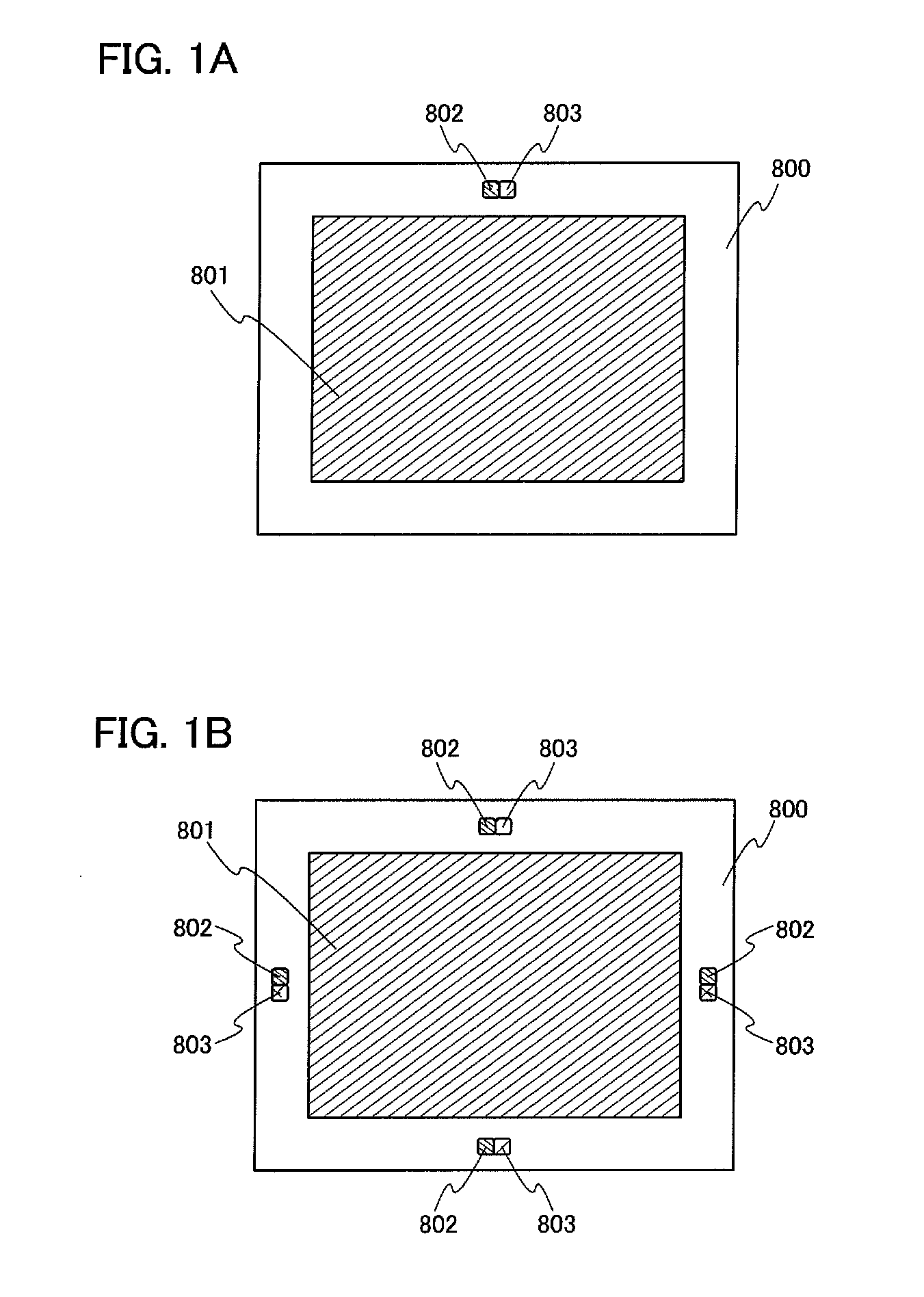
[0049]In this embodiment, one embodiment of a display device incorporating an optical sensor will be described. FIGS. 1A and 1B each illustrate a display device 800 incorporating an optical sensor. In FIG. 1A, an optical sensor 802 and an optical sensor 803 are provided in an upper portion outside a display portion 801. In FIG. 1B, a plurality of optical sensors 802 and a plurality of optical sensors 803 are provided around a display portion 801.

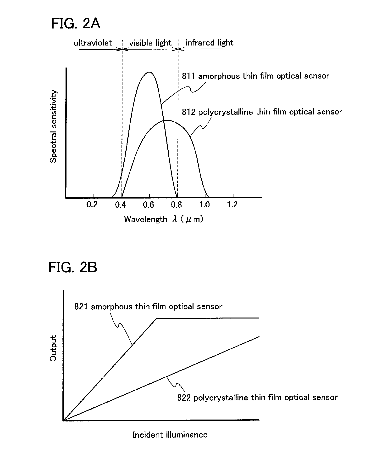
[0050]In the optical sensor 802, a photoelectric conversion element includes an amorphous semiconductor, and in the optical sensor 803, a photoelectric conversion element includes a polycrystalline semiconductor. The illuminance around the display device is detected by the optical sensor 802 or the optical sensor 803, and the luminance of the display device is adjusted. For example, when the illuminance around the display device is high, the luminance of the display portion 801 is increased, and when the illuminance around the di...

Example

Embodiment 2

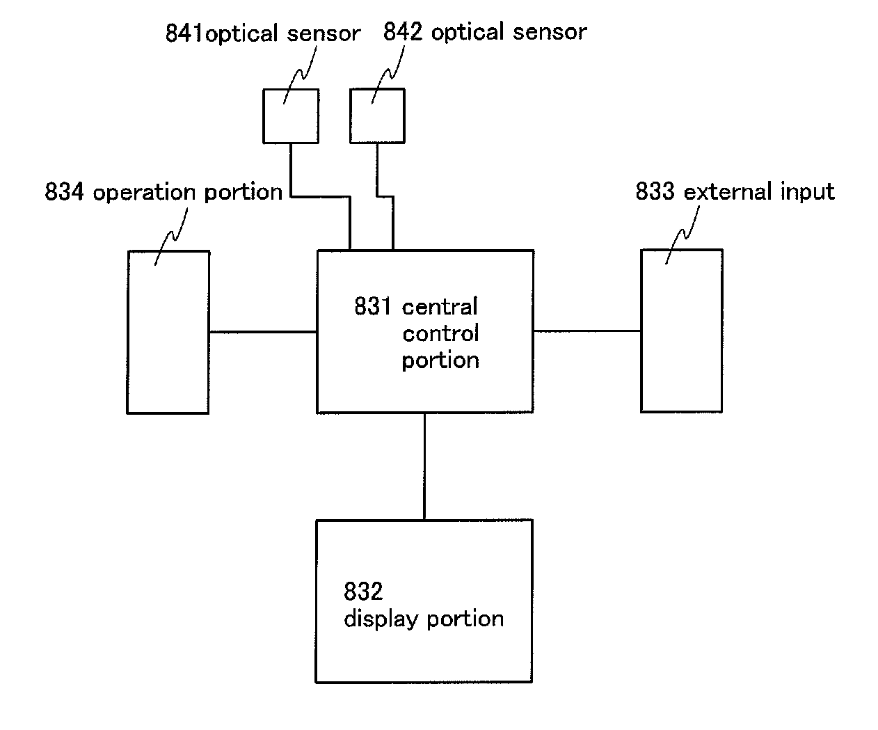
[0070]In this embodiment, an embodiment of a display device incorporating an optical sensor, which is different from Embodiment 1, will be described.

[0071]In this embodiment, as an example of a display device, a liquid crystal display device will be described with reference to FIG. 4. A display device 220 includes a pixel circuit 221, a display element control circuit 222, and an optical sensor control circuit 223. The pixel circuit 221 has a plurality of pixels 224 arranged in matrix. Each of the pixels 224 includes a display element 225 and an optical sensor 226 or an optical sensor 236.

[0072]The optical sensor 226 is the amorphous thin film optical sensor described in Embodiment 1, and the optical sensor 236 is the polycrystalline thin film optical sensor. FIG. 4 illustrates an example where columns of pixels each including the optical sensor 226 and columns of pixels each including the optical sensor 236 are alternately arranged one by one; however, this embodiment i...

Example

Embodiment 3

[0102]In this embodiment, an example of a manufacturing process of the transistor and the optical sensor described in Embodiments 1 and 2 will be described with reference to cross-sectional views of FIGS. 8A to 8D, FIGS. 9A to 9D, FIGS. 10A and 10B, and FIG. 11. A transistor 390 illustrated in FIG. 10B is one type of bottom-gate structures and is also referred to as an inverted-staggered transistor or a channel-etched transistor. An optical sensor 391 is an amorphous thin film optical sensor and includes a PIN photodiode in which a P layer, an I layer, and an N layer formed with amorphous silicon are stacked. An optical sensor 392 is a polycrystalline thin film optical sensor and includes a PIN photodiode in which a P layer, an I layer, and an N layer are formed in one polycrystalline silicon or microcrystalline silicon layer as a photoelectric conversion element. Note that the optical sensor 391 and the optical sensor 392 are designed to detect not light incident from t...


PUM


Abstract

An object is to provide a display device with low power consumption and good display quality. A first substrate is provided with a terminal portion, a pixel electrode, a switching transistor including an oxide semiconductor, a first optical sensor having high optical sensitivity to visible light, and a second optical sensor having optical sensitivity to infrared light and having lower optical sensitivity to visible light than the first optical sensor. The illuminance or color temperature around a display device is detected using the first and second optical sensors, and the luminance or color tone of a display image is adjusted. A second substrate is provided so as to face the first substrate, and is provided with a counter electrode. In a period for displaying a still image, the switching transistor is turned off so that the counter electrode is brought into a floating state.

Description

TECHNICAL FIELD[0001]An embodiment of the present invention relates to an optical sensor including a thin film semiconductor, and to a display device including the optical sensor.BACKGROUND ART[0002]In recent years, there has been a trend in active matrix display devices typified by a liquid crystal display device towards a larger screen of a diagonal size of 20 inches or more, and further, the development of an active matrix display device is aimed even at a diagonal screen size of 100 inches or more. In addition, there is a trend toward higher screen resolution, e.g., high-definition (HD) image quality (1366×768) or full high-definition (FHD) image quality (1920×1080), and the development of a so-called 4K Digital Cinema display device, which has a resolution of 3840×2048 or 4096×2180, is also accelerated.[0003]As the screen size or resolution increases, a transistor is required to have higher field effect mobility. In addition, as the screen size increases, not only does power co...

Claims


Application Information

Patent Timeline
IPC IPC(8): G09G3/36G09G5/00
CPCG02F1/13318G02F1/1368G02F2001/13312G09G3/3225G09G2360/144G09G2310/0235G09G2320/0295G09G2320/0626G09G3/3648G02F1/13312G09F27/005G09G3/2003G09G3/3413G09G3/3696G09G2300/0426G09G2310/0202G09G2320/0666G09G2330/021G09G2360/14
Inventor YAMAZAKI, SHUNPEI
Owner SEMICON ENERGY LAB CO LTD
Why Eureka
Try Eureka